
DDR2 Memory Controller User's Guide

www.ti.com
4.5 SDRAM Timing 1 Register (SDTIM1)
DDR2 Memory Controller Registers
The SDRAM timing 1 register (SDTIM1) configures the DDR2 memory controller to meet many of the AC
timing specification of the DDR2 memory. Note that DDR_CLK is equal to the period of the DDR_CLK
signal. See the DDR2 memory data sheet for information on the appropriate values to program each field.
The bit fields in the SDTIM1 register are only writeable when the TIMUNLOCK bit of the SDRAM
Configuration register (SDCFG) is unlocked. The SDTIM1 is shown in Figure 24 and described in
Table 22 .
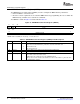
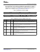
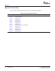
Figure 24. SDRAM Timing 1 Register (SDTIM1)
31 25 24 22 21 19 18 16
T_RFC T_RP T_RCD T_WR
R/W-0x3F R/W-0x7 R/W-0x7 R/W-0x7
15 11 10 6 5 3 2 1 0
T_RAS T_RC T_RRD Rsvd T_WTR
R/W-0x1F R/W-0x1F R/W-0x7 R-0 R/W-0x3
LEGEND: R/W = Read/Write; R = Read only; - n = value after reset
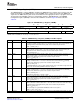
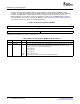
Table 22. SDRAM Timing 1 Register (SDTIM1) Field Descriptions
Bit Field Value Description
31-25 T_RFC These bits specify the minimum number of DDR_CLK cycles from a refresh or load mode command
to a refresh or activate command, minus one. The value for these bits can be derived from the t
rfc
AC timing parameter in the DDR2 memory data sheet. Calculate using this formula:
T_RFC = (t
rfc
/DDR_CLK) - 1
24-22 T_RP These bits specify the minimum number of DDR_CLK cycles from a precharge command to a
refresh or activate command, minus 1. The value for these bits can be derived from the t
rp
AC
timing parameter in the DDR2 memory data sheet. Calculate using the formula:
T_RP = (t
rp
/DDR_CLK) - 1
21-19 T_RCD These bits specify the minimum number of DDR_CLK cycles from an activate command to a read
or write command, minus 1. The value for these bits can be derived from the t
rcd
AC timing
parameter in the DDR2 memory data sheet. Calculate using the formula:
T_RCD = (t
rcd
/DDR_CLK) - 1
18-16 T_WR These bits specify the minimum number of DDR_CLK cycles from the last write transfer to a
precharge command, minus 1. The value for these bits can be derived from the t
wr
AC timing
parameter in the DDR2 memory data sheet. Calculate using the formula:
T_WR = (t
wr
/DDR_CLK) - 1
The SDRAM initialization sequence will be started when the value of this field is changed from the
previous value and the DDR2_ENABLE in SDCFG is equal to 1.
15-11 T_RAS These bits specify the minimum number of DDR_CLK cycles from an activate command to a
precharge command, minus 1. The value for these bits can be derived from the t
ras
AC timing
parameter in the DDR2 memory data sheet. Calculate using this formula:
T_RAS = (t
ras
/DDR_CLK) - 1
T_RAS must be greater than or equal to T_RCD.
10-6 T_RC These bits specify the minimum number of DDR_CLK cycles from an activate command to an
activate command, minus 1. The value for these bits can be derived from the t
rc
AC timing
parameter in the DDR2 memory data sheet. Calculate using this formula:
T_RC = (t
rc
/DDR_CLK) - 1
5-3 T_RRD These bits specify the minimum number of DDR_CLK cycles from an activate command to an
activate command in a different bank, minus 1. The value for these bits can be derived from the t
rrd
AC timing parameter in the DDR2 memory data sheet. Calculate using this formula:
T_RRD = (t
rrd
/DDR_CLK) - 1
When connecting to an 8_bank DDR2 SDRAM, this field must be equal to:
T_RRD = ( (4*t
rrd
+ 2*t
ck
) / (4*t
ck
) ) - 1
2 Reserved Reserved. The reserved bit location is always read as 0. A value written to this field has no effect.
SPRUEK5A – October 2007 DSP DDR2 Memory Controller 41
Submit Documentation Feedback