
Video Port/VCXO Interpolated Control (VIC) Port User's Guide

www.ti.com
4.12 Video Display Registers
4.12.1 Video Display Status Register (VDSTAT)
Video Display Registers
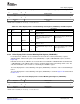
The registers for controlling the video display mode of operation are listed in Table 4-5 . See the
device-specific datasheet for the memory address of these registers.
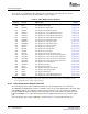
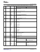
Table 4-5. Video Display Control Registers
Offset
Address
(1)
Acronym Register Name Section
200h VDSTAT Video Display Status Register Section 4.12.1
204h VDCTL Video Display Control Register Section 4.12.2
208h VDFRMSZ Video Display Frame Size Register Section 4.12.3
20Ch VDHBLNK Video Display Horizontal Blanking Register Section 4.12.4
210h VDVBLKS1 Video Display Field 1 Vertical Blanking Start Register Section 4.12.5
214h VDVBLKE1 Video Display Field 1 Vertical Blanking End Register Section 4.12.6
218h VDVBLKS2 Video Display Field 2 Vertical Blanking Start Register Section 4.12.7
21Ch VDVBLKE2 Video Display Field 2 Vertical Blanking End Register Section 4.12.8
220h VDIMGOFF1 Video Display Field 1 Image Offset Register Section 4.12.9
224h VDIMGSZ1 Video Display Field 1 Image Size Register Section 4.12.10
228h VDIMGOFF2 Video Display Field 2 Image Offset Register Section 4.12.11
22Ch VDIMGSZ2 Video Display Field 2 Image Size Register Section 4.12.12
230h VDFLDT1 Video Display Field 1 Timing Register Section 4.12.13
234h VDFLDT2 Video Display Field 2 Timing Register Section 4.12.14
238h VDTHRLD Video Display Threshold Register Section 4.12.15
23Ch VDHSYNC Video Display Horizontal Synchronization Register Section 4.12.16
240h VDVSYNS1 Video Display Field 1 Vertical Synchronization Start Register Section 4.12.17
244h VDVSYNE1 Video Display Field 1 Vertical Synchronization End Register Section 4.12.18
248h VDVSYNS2 Video Display Field 2 Vertical Synchronization Start Register Section 4.12.19
24Ch VDVSYNE2 Video Display Field 2 Vertical Synchronization End Register Section 4.12.20
250h VDRELOAD Video Display Counter Reload Register Section 4.12.21
254h VDDISPEVT Video Display Event Register Section 4.12.22
258h VDCLIP Video Display Clipping Register Section 4.12.23
25Ch VDDEFVAL Video Display Default Display Value Register Section 4.12.24
260h VDVINT Video Display Vertical Interrupt Register Section 4.12.25
264h VDFBIT Video Display Field Bit Register Section 4.12.26
268h VDVBIT1 Video Display Field 1 Vertical Blanking Bit Register Section 4.12.27
26Ch VDVBIT2 Video Display Field 2 Vertical Blanking Bit Register Section 4.12.28
(1)
The absolute address of the registers is device/port specific and is equal to the base address + offset address. See the
device-specific datasheet to verify the register addresses.
The video display status register (VDSTAT) indicates the current display status of the video port.
The VDXPOS and VDYPOS bits track the coordinates of the most-recently displayed pixel. The F1D, F2D,
and FRMD bits indicate the completion of fields or frames and may need to be cleared by the DSP to
prevent a DCNA interrupt from being generated, depending on the selected frame operation. The F1D,
F2D, and FRMD bits are set when the final pixel from the appropriate field has been sent to the output
pad.
The video display status register (VDSTAT) is shown in Figure 4-31 and described in Table 4-6 .
Video Display Port122 SPRUEM1 – May 2007
Submit Documentation Feedback