
Video Port/VCXO Interpolated Control (VIC) Port User's Guide

www.ti.com
Video Display Registers
The video display is controlled by the video display control register (VDCTL).
The video display control register (VDCTL) is shown in Figure 4-32 and described in Table 4-7 .
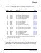
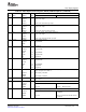
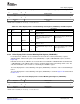
Figure 4-32. Video Display Control Register (VDCTL)
31 30 29 28 27 24
RSTCH BLKDIS Reserved PVPSYN Reserved
R/WS-0 R/W-1 R-0 R/W-0 R-0
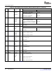
23 22 21 20 19 18 17 16
FXS VXS HXS VCTL3S VCTL2S VCTL1S
R/W-0 R/W-0 R/W-0 R/W-0 R/W-0 R/W-0
15 14 13 12 11 10 9 8
VDEN Reserved RGBX RSYNC DVEN RESMPL Reserved SCALE
R/W-0 R-0 R/W-0 R/W-0 R/W-0 R/W-0 R-0 R/W-0
7 6 5 4 3 2 0
CON FRAME DF2 DF1 Reserved DMODE
R/W-0 R/W-0 R/W-0 R/W-0 R-0 R/W-0
LEGEND: R/W = Read/Write; R = Read only; - n = value after reset
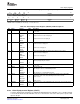
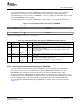
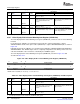
Table 4-7. Video Display Control Register (VDCTL) Field Descriptions
Description
Bit field
(1)
symval
(1)
Value BT.656 and Y/C Mode Raw Data Mode
31 RSTCH OF( value) Reset channel bit. Write 1 to reset the bit, a write of 0 has no effect. 0 1
DEFAULT 0 No effect.
NONE
RESET 1 Resets the video display module and sets its registers to their initial values. Also
clears the VDEN bit. The video display module automatically clears RSTCH after
software reset is completed.
30 BLKDIS OF( value) Block display events bit. BLKDIS functions as a display FIFO reset without affecting
the current programmable register values.
The video display module continues to function normally, the counters count, control
outputs are generated, EAV/SAV codes are generated for BT.656 and Y/C modes,
and default or blanking data is output during active display time. No data is moved to
the display FIFOs because no events occur. The F1D, F2D, and FRMD bits in
VDSTAT are still set when fields or frames are complete.
CLEAR 0 Clearing BLKDIS does not enable EDMA events during the field in which the bit is
cleared. EDMA events are enabled at the start of the next frame after the one in
which the bit is cleared. This allows the EDMA to always be synced to the proper
field.
DEFAULT 1 Blocks EDMA events and flushes the display FIFOs.
BLOCK
29 Reserved - 0 The reserved bit location is always read as 0. A value written to this field has no
effect.
28 PVPSYN OF( value) Previous video port synchronization enable bit. 0
DEFAULT 0
DISABLE
ENABLE 1 Output timing is locked to preceding video port (VP2 is locked to VP1 or VP1 is
locked to VP0, see Figure 4-7 .
27-24 Reserved - 0 Reserved. The reserved bit location is always read as 0. A value written to this field
has no effect.
(1)
For CSL implementation, use the notation VP_VDCTL_ field_ symval
124 Video Display Port SPRUEM1 – May 2007
Submit Documentation Feedback