
Video Port/VCXO Interpolated Control (VIC) Port User's Guide


www.ti.com
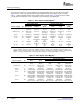
1.4.2 VDOUT Data Bus Usage for Display Modes
1.5 Video Port Pin Multiplexing
1.6 VideoPort Clocking
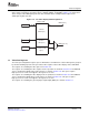
Video Port Pin Multiplexing
The alignment and usage of data on the VDOUT bus depends on the display mode as shown in
Table 1-4 .
Table 1-4. VDOUT Data Bus Usage for Display Modes
(1)
Display Mode
BT.656 Y/C Dual Sync Raw Data Raw Data
Data Bus 8-Bit 8-Bit 8-Bit 16-Bit
VDOUT19 A (C) (B) A
VDOUT18 A (C) (B) A
VDOUT17 A (C) (B) A
VDOUT16 A (C) (B) A
VDOUT15 A (C) (B) A
VDOUT14 A (C) (B) A
VDOUT13 A (C) (B) A
VDOUT12 A (C) (B) A
VDOUT9 A A (Y) A A
VDOUT8 A A (Y) A A
VDOUT7 A A (Y) A A
VDOUT6 A A (Y) A A
VDOUT5 A A (Y) A A
VDOUT4 A A (Y) A A
VDOUT3 A A (Y) A A
VDOUT2 A A (Y) A A
(1)
Legend: A – Channel A display; A(C) Channel A chroma; A(Y) Channel A luma; B – Optional locked channel B display
None of the five Video Port have dedicated pins associated with them. Each of the Video Port has its pins
multiplexed with other peripherals. In order to use a desired Video Port either in Capture or Display Mode,
the user would first need to program the Pin Mux Register (PINMUX) appropriately to ensure that the
multiplexed pins work as VideoPort pins. Refer to the device-specific data manual to know details of the
PINMUX Register.
Each of the Video Ports have a LPSC associated with them. The LPSC provides the module clock and
reset control. On power up, the LPSC's associated with Video Ports do not gate the clock required for the
Video Port to function. User would need to appropriately program the LPSC associated with Video Port to
provide the clock to the desired Video Port before trying a data transfer operation. Refer to the
device-specific manual to know LPSC Video Port association and details of LPSC registers.
28 Overview SPRUEM1 – May 2007
Submit Documentation Feedback