
Video Port/VCXO Interpolated Control (VIC) Port User's Guide

www.ti.com
2.4.1 Video Port Control Register (VPCTL)
Video Port Control Registers
The video port control register (VPCTL) determines the basic operation of the video port.
Not all combinations of the port control bits are unique. The control bit encoding is shown in Table 2-3 .
Additional mode options are selected using the video capture channel A control register (VCACTL) and
video display control register (VDCTL).
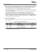
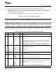
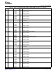
The video port control register (VPCTL) is shown in Figure 2-1 and described in Table 2-2 .
Figure 2-1. Video Port Control Register (VPCTL)
31 16
Reserved
R-0
15 14 13 8
VPRST VPHLT Reserved
R/WS-0 R/WC-1 R-0
7 6 5 4 3 2 1 0
VCLK2P VCT3P VCT2P VCT1P Reserved TCI DISP DCHNL
R/W-0 R/W-0 R/W-0 R/W-0 R-0 R/W-0 R/W-0 R/W-0
LEGEND: R/W = Read/Write; R = Read only; WC = Write a 1 to clear; WS = Write 1 to set, a write of 0 has no effect; - n = value after reset
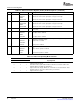
Table 2-2. Video Port Control Register (VPCTL) Field Descriptions
Bit field
(1)
symval
(1)
Value Description
31-16 Reserved - 0 Reserved. The reserved bit location is always read as 0. A value written to this field
has no effect.
15 VPRST OF( value) Video port software reset enable bit. VPRST is set by writing a 1. Writing 0 has no
effect.
DEFAULT 0 No effect.
NO
RESET 1 Flush all FIFOs and set all port registers to their initial values. VCLK1 and VCLK2 are
configured as inputs and all VDATA and VCTL pins are placed in high impedance.
Auto-cleared after reset is complete.
The VPRST bit may take several clock cycles to clear to 0. The VPRST bit should be
polled to make sure the bit is cleared prior to writing to the video port registers.
14 VPHLT OF( value) Video port halt bit. This bit is set upon hardware or software reset. The other VPCTL
bits (except VPRST) can only be changed when VPHLT is 1. VPHLT is cleared by
writing a 1. Writing 0 has no effect.
NONE 0 No effect.
DEFAULT 1 VPHLT is cleared.
CLEAR
13-6 Reserved - 0 Reserved. The reserved bit location is always read as 0. A value written to this field
has no effect.
7 VCLK2P OF( value) VCLK2 pin polarity bit. Has no effect in capture mode.
DEFAULT 0
NONE
REVERSE 1 Inverts the VCLK2 output clock polarity in display mode.
6 VCT3P OF( value) VCTL3 pin polarity. Does not affect GPIO operation. If VCTL3 pin is used as a FLD
input on the video capture side, then the VCTL3 polarity is not considered; the field
inverse is controlled by the FINV bit in the video capture channel x control register
(VC xCTL).
DEFAULT 0 Indicates the VCTL3 control signal (input or output) is active high.
NONE
ACTIVELOW 1 Indicates the VCTL3 control signal (input or output) is active low.
(1)
For CSL implementation, use the notation VP_VPCTL_ field_ symval
SPRUEM1 – May 2007 Video Port 35
Submit Documentation Feedback