
Video Port/VCXO Interpolated Control (VIC) Port User's Guide

www.ti.com
BT.656 Video Capture Mode
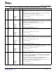
Table 3-2. BT.656 Video Timing Reference Codes
Data Bit 1
st
Byte (FFh) 2
nd
Byte (00h) 3
rd
Byte (00h) 4
th
Byte (XYh)
9 (MSB) 1 0 0 1
8 1 0 0 F (field)
(1)
7 1 0 0 V (vertical blanking)
(2)
6 1 0 0 H (horizontal blanking)
(3)
5 1 0 0 P3 (protection bit 3)
(4)
4 1 0 0 P2 (protection bit 2)
(4)
3 1 0 0 P1 (protection bit 1)
(4)
2 1 0 0 P0 (protection bit 0)
(4)
(1)
F = 0 during Field 1; F = 1 during Field 2
(2)
V = 0 elsewhere; V = 1 during field blanking
(3)
H = 0 in SAV; H = 1 in EAV
(4)
P0, P1, P2, and P3: Depends on F, V, and H state.
Bits P0, P1, P2, and P3 have different states depending on the state of bits F, V, and H as shown in
Table 3-3 .
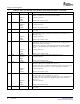
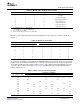
Table 3-3. BT.656 Protection Bits
Line Information Bits Protection Bits
F V H P3 P2 P1 P0
0 0 0 0 0 0 0
0 0 1 1 1 0 1
0 1 0 1 0 1 1
0 1 1 0 1 1 0
1 0 0 0 1 1 1
1 0 1 1 0 1 0
1 1 0 1 1 0 0
1 1 1 0 0 0 1
The protection bits allow the port to implement a DEDSEC (double error detection, single error correction)
function on the received video timing reference code. The corrected values for the F, H, and V bits based
on the protection bit values are shown in Table 3-4 . The - entries indicate detected double bit errors that
cannot be corrected. Detection of these errors causes the SERR x bit in the video port interrupt status
register (VPIS) to be set.
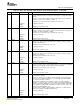
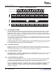
Table 3-4. Error Correction by Protection Bits
Received F, V, and H Bits
Received P
3
-P
0
Bits 000 001 010 011 100 101 110 111
0000 000 000 000 - 000 - - 111
0001 000 - - 111 - 111 111 111
0010 000 - - 011 - 101 - -
0011 - - 010 - 100 - - 111
0100 000 - - 011 - - 110 -
0101 - 001 - - 100 - - 111
0110 - 011 011 011 100 - - 011
0111 100 - - 011 100 100 100 -
1000 000 - - - - 101 110 -
1001 - 001 010 - - - - 111
1010 - 101 010 - 101 101 - 101
SPRUEM1 – May 2007 Video Capture Port 47
Submit Documentation Feedback