TMS320F28027, TMS320F28026, TMS320F28023, TMS320F28022 TMS320F28021, TMS320F28020, TMS320F280200 www.ti.com SPRS523J – NOVEMBER 2008 – REVISED OCTOBER 2013 Piccolo™ Microcontrollers Check for Samples: TMS320F28027, TMS320F28026, TMS320F28023, TMS320F28022, TMS320F28021, TMS320F28020, TMS320F280200 1 TMS320F2802x, TMS320F2802xx (Piccolo) MCUs 1.1 Features 1234 • High-Efficiency 32-Bit CPU ( TMS320C28x™) – 60 MHz (16.
TMS320F28027, TMS320F28026, TMS320F28023, TMS320F28022 TMS320F28021, TMS320F28020, TMS320F280200 SPRS523J – NOVEMBER 2008 – REVISED OCTOBER 2013 1.2 • • • • • • • • www.ti.com Applications White Goods Switch Mode Power Supplies (SMPSs) DC-DC Multiple-Output Power Supplies Solar Micro Inverters and Converters LED Lighting Power Factor Correction Sewing and Textile Machines eBikes 1.
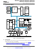
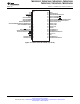
TMS320F28027, TMS320F28026, TMS320F28023, TMS320F28022 TMS320F28021, TMS320F28020, TMS320F280200 www.ti.com 1.4 SPRS523J – NOVEMBER 2008 – REVISED OCTOBER 2013 Functional Block Diagram Figure 1-1 shows the functional block diagram for the device.
TMS320F28027, TMS320F28026, TMS320F28023, TMS320F28022 TMS320F28021, TMS320F28020, TMS320F280200 SPRS523J – NOVEMBER 2008 – REVISED OCTOBER 2013 1 TMS320F2802x, TMS320F2802xx (Piccolo) MCUs 1 ............................................. 1 1.2 Applications .......................................... 2 1.3 Description ........................................... 2 1.4 Functional Block Diagram ........................... 3 1.5 Getting Started ....................................... 3 Revision History .......
TMS320F28027, TMS320F28026, TMS320F28023, TMS320F28022 TMS320F28021, TMS320F28020, TMS320F280200 www.ti.com SPRS523J – NOVEMBER 2008 – REVISED OCTOBER 2013 Revision History NOTE: Page numbers for previous revisions may differ from page numbers in the current version. This data manual revision history highlights the technical changes made to the SPRS523I device-specific data manual to make it an SPRS523J revision. Scope: See table below. LOCATION Section 1 Section 1.
TMS320F28027, TMS320F28026, TMS320F28023, TMS320F28022 TMS320F28021, TMS320F28020, TMS320F280200 SPRS523J – NOVEMBER 2008 – REVISED OCTOBER 2013 www.ti.com 2 Introduction Table 2-1 lists the features of the TMS320F2802x devices.
TMS320F28027, TMS320F28026, TMS320F28023, TMS320F28022 TMS320F28021, TMS320F28020, TMS320F280200 www.ti.com SPRS523J – NOVEMBER 2008 – REVISED OCTOBER 2013 Table 2-1.
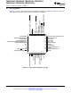
TMS320F28027, TMS320F28026, TMS320F28023, TMS320F28022 TMS320F28021, TMS320F28020, TMS320F280200 SPRS523J – NOVEMBER 2008 – REVISED OCTOBER 2013 2.1 www.ti.com Pin Assignments 36 35 34 33 32 31 30 29 28 27 26 25 GPIO33/SCLA/EPWMSYNCO/ADCSOCBO VDDIO VREGENZ VSS VDD GPIO32/SDAA/EPWMSYNCI/ADCSOCAO TEST GPIO0/EPWM1A GPIO1/EPWM1B/COMP1OUT GPIO16/SPISIMOA/TZ2 GPIO17/SPISOMIA/TZ3 GPIO19/XCLKIN/SPISTEA/SCIRXDA/ECAP1 Figure 2-1 shows the 48-pin PT low-profile quad flatpack (LQFP) pin assignments.
TMS320F28027, TMS320F28026, TMS320F28023, TMS320F28022 TMS320F28021, TMS320F28020, TMS320F280200 www.ti.
TMS320F28027, TMS320F28026, TMS320F28023, TMS320F28022 TMS320F28021, TMS320F28020, TMS320F280200 SPRS523J – NOVEMBER 2008 – REVISED OCTOBER 2013 2.2 www.ti.com Signal Descriptions Table 2-2 describes the signals. With the exception of the JTAG pins, the GPIO function is the default at reset, unless otherwise mentioned. The peripheral signals that are listed under them are alternate functions. Some peripheral functions may not be available in all devices. See Table 2-1 for details.
TMS320F28027, TMS320F28026, TMS320F28023, TMS320F28022 TMS320F28021, TMS320F28020, TMS320F280200 www.ti.com SPRS523J – NOVEMBER 2008 – REVISED OCTOBER 2013 Table 2-2. Terminal Functions(1) (continued) TERMINAL PT PIN # DA PIN # I/O/Z X1 45 – I On-chip crystal-oscillator input. To use this oscillator, a quartz crystal or a ceramic resonator must be connected across X1 and X2. In this case, the XCLKIN path must be disabled by bit 13 in the CLKCTL register.
TMS320F28027, TMS320F28026, TMS320F28023, TMS320F28022 TMS320F28021, TMS320F28020, TMS320F280200 SPRS523J – NOVEMBER 2008 – REVISED OCTOBER 2013 www.ti.com Table 2-2. Terminal Functions(1) (continued) TERMINAL PT PIN # DA PIN # VDDA 11 22 VSSA VREFLO 12 23 VDD 32 1 VDD 43 11 VDDIO 35 4 VSS 33 2 VSS 44 12 NAME I/O/Z DESCRIPTION CPU AND I/O POWER Analog Power Pin. Tie with a 2.2-µF capacitor (typical) close to the pin.
TMS320F28027, TMS320F28026, TMS320F28023, TMS320F28022 TMS320F28021, TMS320F28020, TMS320F280200 www.ti.com SPRS523J – NOVEMBER 2008 – REVISED OCTOBER 2013 Table 2-2.
TMS320F28027, TMS320F28026, TMS320F28023, TMS320F28022 TMS320F28021, TMS320F28020, TMS320F280200 SPRS523J – NOVEMBER 2008 – REVISED OCTOBER 2013 www.ti.com Table 2-2.
TMS320F28027, TMS320F28026, TMS320F28023, TMS320F28022 TMS320F28021, TMS320F28020, TMS320F280200 www.ti.com SPRS523J – NOVEMBER 2008 – REVISED OCTOBER 2013 3 Functional Overview 3.1 Memory Maps In Figure 3-1, Figure 3-2, Figure 3-3, Figure 3-4, and Figure 3-5, the following apply: • Memory blocks are not to scale. • Peripheral Frame 0, Peripheral Frame 1 and Peripheral Frame 2 memory maps are restricted to data memory only. A user program cannot access these memory maps in program space.
TMS320F28027, TMS320F28026, TMS320F28023, TMS320F28022 TMS320F28021, TMS320F28020, TMS320F280200 SPRS523J – NOVEMBER 2008 – REVISED OCTOBER 2013 www.ti.
TMS320F28027, TMS320F28026, TMS320F28023, TMS320F28022 TMS320F28021, TMS320F28020, TMS320F280200 www.ti.
TMS320F28027, TMS320F28026, TMS320F28023, TMS320F28022 TMS320F28021, TMS320F28020, TMS320F280200 SPRS523J – NOVEMBER 2008 – REVISED OCTOBER 2013 www.ti.
TMS320F28027, TMS320F28026, TMS320F28023, TMS320F28022 TMS320F28021, TMS320F28020, TMS320F280200 www.ti.
TMS320F28027, TMS320F28026, TMS320F28023, TMS320F28022 TMS320F28021, TMS320F28020, TMS320F280200 SPRS523J – NOVEMBER 2008 – REVISED OCTOBER 2013 www.ti.
TMS320F28027, TMS320F28026, TMS320F28023, TMS320F28022 TMS320F28021, TMS320F28020, TMS320F280200 www.ti.com SPRS523J – NOVEMBER 2008 – REVISED OCTOBER 2013 Table 3-1.
TMS320F28027, TMS320F28026, TMS320F28023, TMS320F28022 TMS320F28021, TMS320F28020, TMS320F280200 SPRS523J – NOVEMBER 2008 – REVISED OCTOBER 2013 www.ti.com Table 3-4.
TMS320F28027, TMS320F28026, TMS320F28023, TMS320F28022 TMS320F28021, TMS320F28020, TMS320F280200 www.ti.com 3.2 3.2.1 SPRS523J – NOVEMBER 2008 – REVISED OCTOBER 2013 Brief Descriptions CPU The 2802x (C28x) family is a member of the TMS320C2000™ microcontroller (MCU) platform. The C28xbased controllers have the same 32-bit fixed-point architecture as existing C28x MCUs.
TMS320F28027, TMS320F28026, TMS320F28023, TMS320F28022 TMS320F28021, TMS320F28020, TMS320F280200 SPRS523J – NOVEMBER 2008 – REVISED OCTOBER 2013 3.2.4 www.ti.com Real-Time JTAG and Analysis The devices implement the standard IEEE 1149.1 JTAG (1) interface for in-circuit based debug. Additionally, the devices support real-time mode of operation allowing modification of the contents of memory, peripheral, and register locations while the processor is running and executing code and servicing interrupts.
TMS320F28027, TMS320F28026, TMS320F28023, TMS320F28022 TMS320F28021, TMS320F28020, TMS320F280200 www.ti.com 3.2.8 SPRS523J – NOVEMBER 2008 – REVISED OCTOBER 2013 Boot ROM The Boot ROM is factory-programmed with boot-loading software. Boot-mode signals are provided to tell the bootloader software what boot mode to use on power up. The user can select to boot normally or to download new software from an external connection or to select boot software that is programmed in the internal Flash/ROM.
TMS320F28027, TMS320F28026, TMS320F28023, TMS320F28022 TMS320F28021, TMS320F28020, TMS320F280200 SPRS523J – NOVEMBER 2008 – REVISED OCTOBER 2013 3.2.9 www.ti.com Security The devices support high levels of security to protect the user firmware from being reverse engineered. The security features a 128-bit password (hardcoded for 16 wait-states), which the user programs into the flash. One code security module (CSM) is used to protect the flash/OTP and the L0/L1 SARAM blocks.
TMS320F28027, TMS320F28026, TMS320F28023, TMS320F28022 TMS320F28021, TMS320F28020, TMS320F280200 www.ti.
TMS320F28027, TMS320F28026, TMS320F28023, TMS320F28022 TMS320F28021, TMS320F28020, TMS320F280200 SPRS523J – NOVEMBER 2008 – REVISED OCTOBER 2013 www.ti.com 3.2.14 Peripheral Clocking The clocks to each individual peripheral can be enabled/disabled to reduce power consumption when a peripheral is not in use. Additionally, the system clock to the serial ports (except I2C) can be scaled relative to the CPU clock. 3.2.15 Low-power Modes The devices are full static CMOS devices.
TMS320F28027, TMS320F28026, TMS320F28023, TMS320F28022 TMS320F28021, TMS320F28020, TMS320F280200 www.ti.com SPRS523J – NOVEMBER 2008 – REVISED OCTOBER 2013 3.2.17 General-Purpose Input/Output (GPIO) Multiplexer Most of the peripheral signals are multiplexed with general-purpose input/output (GPIO) signals. This enables the user to use a pin as GPIO if the peripheral signal or function is not used. On reset, GPIO pins are configured as inputs.
TMS320F28027, TMS320F28026, TMS320F28023, TMS320F28022 TMS320F28021, TMS320F28020, TMS320F280200 SPRS523J – NOVEMBER 2008 – REVISED OCTOBER 2013 www.ti.com 3.2.20 Serial Port Peripherals The devices support the following serial communication peripherals: 30 SPI: The SPI is a high-speed, synchronous serial I/O port that allows a serial bit stream of programmed length (one to sixteen bits) to be shifted into and out of the device at a programmable bit-transfer rate.
TMS320F28027, TMS320F28026, TMS320F28023, TMS320F28022 TMS320F28021, TMS320F28020, TMS320F280200 www.ti.com 3.3 SPRS523J – NOVEMBER 2008 – REVISED OCTOBER 2013 Register Map The devices contain three peripheral register spaces. The spaces are categorized as follows: Peripheral Frame 0: These are peripherals that are mapped directly to the CPU memory bus. See Table 3-8. Peripheral Frame 1: These are peripherals that are mapped to the 32-bit peripheral bus. See Table 3-9.
TMS320F28027, TMS320F28026, TMS320F28023, TMS320F28022 TMS320F28021, TMS320F28020, TMS320F280200 SPRS523J – NOVEMBER 2008 – REVISED OCTOBER 2013 3.4 www.ti.com Device Emulation Registers These registers are used to control the protection mode of the C28x CPU and to monitor some critical device signals. The registers are defined in Table 3-11 . Table 3-11.
TMS320F28027, TMS320F28026, TMS320F28023, TMS320F28022 TMS320F28021, TMS320F28020, TMS320F280200 www.ti.com 3.5 SPRS523J – NOVEMBER 2008 – REVISED OCTOBER 2013 Interrupts Figure 3-6 shows how the various interrupt sources are multiplexed.
TMS320F28027, TMS320F28026, TMS320F28023, TMS320F28022 TMS320F28021, TMS320F28020, TMS320F280200 SPRS523J – NOVEMBER 2008 – REVISED OCTOBER 2013 www.ti.com Eight PIE block interrupts are grouped into one CPU interrupt. In total, 12 CPU interrupt groups, with 8 interrupts per group equals 96 possible interrupts. Table 3-12 shows the interrupts used by 2802x devices. The TRAP #VectorNumber instruction transfers program control to the interrupt service routine corresponding to the vector specified.
TMS320F28027, TMS320F28026, TMS320F28023, TMS320F28022 TMS320F28021, TMS320F28020, TMS320F280200 www.ti.com SPRS523J – NOVEMBER 2008 – REVISED OCTOBER 2013 Table 3-12. PIE MUXed Peripheral Interrupt Vector Table (1) INT1.y INT2.y INT3.y INT4.y INT5.y INT6.y INT7.y INT8.y INT9.y INT10.y INT11.y INT12.y (1) INTx.8 INTx.7 INTx.6 INTx.5 INTx.4 INTx.3 INTx.2 INTx.1 WAKEINT TINT0 ADCINT9 XINT2 XINT1 Reserved ADCINT2 ADCINT1 (LPM/WD) (TIMER 0) (ADC) Ext. int. 2 Ext. int.
TMS320F28027, TMS320F28026, TMS320F28023, TMS320F28022 TMS320F28021, TMS320F28020, TMS320F280200 SPRS523J – NOVEMBER 2008 – REVISED OCTOBER 2013 www.ti.com Table 3-13.
TMS320F28027, TMS320F28026, TMS320F28023, TMS320F28022 TMS320F28021, TMS320F28020, TMS320F280200 www.ti.com 3.5.1 SPRS523J – NOVEMBER 2008 – REVISED OCTOBER 2013 External Interrupts Table 3-14.
TMS320F28027, TMS320F28026, TMS320F28023, TMS320F28022 TMS320F28021, TMS320F28020, TMS320F280200 SPRS523J – NOVEMBER 2008 – REVISED OCTOBER 2013 3.6.2 www.ti.com On-chip Power-On Reset (POR) and Brown-Out Reset (BOR) Circuit Two on-chip supervisory circuits, the power-on reset (POR) and the brown-out reset (BOR) remove the burden of monitoring the VDD and VDDIO supply rails from the application board.
TMS320F28027, TMS320F28026, TMS320F28023, TMS320F28022 TMS320F28021, TMS320F28020, TMS320F280200 www.ti.com 3.7 SPRS523J – NOVEMBER 2008 – REVISED OCTOBER 2013 System Control This section describes the oscillator and clocking mechanisms, the watchdog function and the low power modes. Table 3-15.
TMS320F28027, TMS320F28026, TMS320F28023, TMS320F28022 TMS320F28021, TMS320F28020, TMS320F280200 SPRS523J – NOVEMBER 2008 – REVISED OCTOBER 2013 www.ti.com Figure 3-9 shows the various clock domains that are discussed. Figure 3-10 shows the various clock sources (both internal and external) that can provide a clock for device operation.
TMS320F28027, TMS320F28026, TMS320F28023, TMS320F28022 TMS320F28021, TMS320F28020, TMS320F280200 www.ti.
TMS320F28027, TMS320F28026, TMS320F28023, TMS320F28022 TMS320F28021, TMS320F28020, TMS320F280200 SPRS523J – NOVEMBER 2008 – REVISED OCTOBER 2013 3.7.1 www.ti.com Internal Zero Pin Oscillators The F2802x devices contain two independent internal zero pin oscillators. By default both oscillators are turned on at power up, and internal oscillator 1 is the default clock source at this time. For power savings, unused oscillators may be powered down by the user.
TMS320F28027, TMS320F28026, TMS320F28023, TMS320F28022 TMS320F28021, TMS320F28020, TMS320F280200 www.ti.com 3.7.3 SPRS523J – NOVEMBER 2008 – REVISED OCTOBER 2013 PLL-Based Clock Module The devices have an on-chip, PLL-based clock module. This module provides all the necessary clocking signals for the device, as well as control for low-power mode entry. The PLL has a 4-bit ratio control PLLCR[DIV] to select different CPU clock rates.
TMS320F28027, TMS320F28026, TMS320F28023, TMS320F28022 TMS320F28021, TMS320F28020, TMS320F280200 SPRS523J – NOVEMBER 2008 – REVISED OCTOBER 2013 www.ti.com The PLL-based clock module provides four modes of operation: • INTOSC1 (Internal Zero-pin Oscillator 1): This is the on-chip internal oscillator 1. This can provide the clock for the Watchdog block, core and CPU-Timer 2 • INTOSC2 (Internal Zero-pin Oscillator 2): This is the on-chip internal oscillator 2.
TMS320F28027, TMS320F28026, TMS320F28023, TMS320F28022 TMS320F28021, TMS320F28020, TMS320F280200 www.ti.
TMS320F28027, TMS320F28026, TMS320F28023, TMS320F28022 TMS320F28021, TMS320F28020, TMS320F280200 SPRS523J – NOVEMBER 2008 – REVISED OCTOBER 2013 www.ti.com WDCR (WDPS[2:0]) WDCR (WDDIS) WDCNTR(7:0) WDCLK Watchdog Prescaler /512 WDCLK 8-Bit Watchdog Counter CLR Clear Counter Internal Pullup WDKEY(7:0) Watchdog 55 + AA Key Detector WDRST Generate Output Pulse WDINT (512 OSCCLKs) Good Key XRS Core-reset WDCR (WDCHK[2:0]) WDRST(A) A.
TMS320F28027, TMS320F28026, TMS320F28023, TMS320F28022 TMS320F28021, TMS320F28020, TMS320F280200 www.ti.com 3.8 SPRS523J – NOVEMBER 2008 – REVISED OCTOBER 2013 Low-power Modes Block Table 3-20 summarizes the various modes. Table 3-20.
TMS320F28027, TMS320F28026, TMS320F28023, TMS320F28022 TMS320F28021, TMS320F28020, TMS320F280200 SPRS523J – NOVEMBER 2008 – REVISED OCTOBER 2013 www.ti.com 4 Peripherals 4.1 Analog Block A 12-bit ADC core is implemented that has different timings than the 12-bit ADC used on F280x/F2833x. The ADC wrapper is modified to incorporate the new timings and also other enhancements to improve the timing control of start of conversions.
TMS320F28027, TMS320F28026, TMS320F28023, TMS320F28022 TMS320F28021, TMS320F28020, TMS320F280200 www.ti.com 4.1.1 SPRS523J – NOVEMBER 2008 – REVISED OCTOBER 2013 ADC 4.1.1.1 Features The core of the ADC contains a single 12-bit converter fed by two sample-and-hold circuits. The sampleand-hold circuits can be sampled simultaneously or sequentially. These, in turn, are fed by a total of up to 13 analog input channels.
TMS320F28027, TMS320F28026, TMS320F28023, TMS320F28022 TMS320F28021, TMS320F28020, TMS320F280200 SPRS523J – NOVEMBER 2008 – REVISED OCTOBER 2013 www.ti.com Table 4-1.
TMS320F28027, TMS320F28026, TMS320F28023, TMS320F28022 TMS320F28021, TMS320F28020, TMS320F280200 www.ti.
TMS320F28027, TMS320F28026, TMS320F28023, TMS320F28022 TMS320F28021, TMS320F28020, TMS320F280200 SPRS523J – NOVEMBER 2008 – REVISED OCTOBER 2013 4.1.2 www.ti.com ADC MUX To COMPy A or B input To ADC Channel X Logic implemented in GPIO MUX block AIOx Pin SYSCLK AIOxIN 1 AIOxINE AIODAT Reg (Read) SYNC 0 AIODAT Reg (Latch) AIOxDIR (1 = Input, 0 = Output) AIOMUX 1 Reg AIOSET, AIOCLEAR, AIOTOGGLE Regs AIODIR Reg (Latch) 1 (0 = Input, 1 = Output) 0 0 Figure 4-3.
TMS320F28027, TMS320F28026, TMS320F28023, TMS320F28022 TMS320F28021, TMS320F28020, TMS320F280200 www.ti.com 4.1.3 SPRS523J – NOVEMBER 2008 – REVISED OCTOBER 2013 Comparator Block Figure 4-4 shows the interaction of the Comparator modules with the rest of the system. COMP x A COMP x B + COMP - GPIO MUX TZ1/2/3 COMP x + DAC x Wrapper AIO MUX ePWM COMPxOUT DAC Core 10-Bit Figure 4-4. Comparator Block Diagram Table 4-3.
TMS320F28027, TMS320F28026, TMS320F28023, TMS320F28022 TMS320F28021, TMS320F28020, TMS320F280200 SPRS523J – NOVEMBER 2008 – REVISED OCTOBER 2013 4.2 www.ti.com Serial Peripheral Interface (SPI) Module The device includes the four-pin serial peripheral interface (SPI) module. One SPI module (SPI-A) is available.
TMS320F28027, TMS320F28026, TMS320F28023, TMS320F28022 TMS320F28021, TMS320F28020, TMS320F280200 www.ti.com SPRS523J – NOVEMBER 2008 – REVISED OCTOBER 2013 The SPI port operation is configured and controlled by the registers listed in Table 4-4. Table 4-4.
TMS320F28027, TMS320F28026, TMS320F28023, TMS320F28022 TMS320F28021, TMS320F28020, TMS320F280200 SPRS523J – NOVEMBER 2008 – REVISED OCTOBER 2013 www.ti.com Figure 4-5 is a block diagram of the SPI in slave mode. SPIFFENA SPIFFTX.14 Receiver Overrun Flag RX FIFO Registers SPISTS.7 Overrun INT ENA SPICTL.4 SPIRXBUF RX FIFO _0 RX FIFO _1 ----- SPIINT RX FIFO Interrupt RX FIFO _3 RX Interrupt Logic 16 SPIRXBUF Buffer Register SPIFFOVF FLAG SPIFFRX.
TMS320F28027, TMS320F28026, TMS320F28023, TMS320F28022 TMS320F28021, TMS320F28020, TMS320F280200 www.ti.com 4.3 SPRS523J – NOVEMBER 2008 – REVISED OCTOBER 2013 Serial Communications Interface (SCI) Module The devices include one serial communications interface (SCI) module (SCI-A). The SCI module supports digital communications between the CPU and other asynchronous peripherals that use the standard nonreturn-to-zero (NRZ) format.
TMS320F28027, TMS320F28026, TMS320F28023, TMS320F28022 TMS320F28021, TMS320F28020, TMS320F280200 SPRS523J – NOVEMBER 2008 – REVISED OCTOBER 2013 www.ti.com The SCI port operation is configured and controlled by the registers listed in Table 4-5. Table 4-5.
TMS320F28027, TMS320F28026, TMS320F28023, TMS320F28022 TMS320F28021, TMS320F28020, TMS320F280200 www.ti.com SPRS523J – NOVEMBER 2008 – REVISED OCTOBER 2013 Figure 4-6 shows the SCI module block diagram. SCICTL1.1 SCITXD Frame Format and Mode TXSHF Register Parity Even/Odd Enable TXENA 8 SCICCR.6 SCICCR.5 TX EMPTY SCICTL2.6 TXRDY Transmitter-Data Buffer Register TXWAKE SCICTL1.3 8 TX INT ENA SCICTL2.7 SCICTL2.
TMS320F28027, TMS320F28026, TMS320F28023, TMS320F28022 TMS320F28021, TMS320F28020, TMS320F280200 SPRS523J – NOVEMBER 2008 – REVISED OCTOBER 2013 4.4 www.ti.com Inter-Integrated Circuit (I2C) The device contains one I2C Serial Port. Figure 4-7 shows how the I2C peripheral module interfaces within the device. The I2C module has the following features: • Compliance with the Philips Semiconductors I2C-bus specification (version 2.
TMS320F28027, TMS320F28026, TMS320F28023, TMS320F28022 TMS320F28021, TMS320F28020, TMS320F280200 www.ti.com SPRS523J – NOVEMBER 2008 – REVISED OCTOBER 2013 2 I C Module I2CXSR I2CDXR TX FIFO FIFO Interrupt to CPU/PIE SDA RX FIFO Peripheral Bus I2CRSR SCL I2CDRR Clock Synchronizer Control/Status Registers CPU Prescaler Noise Filters Interrupt to CPU/PIE I2C INT Arbitrator A. B. The I2C registers are accessed at the SYSCLKOUT rate.
TMS320F28027, TMS320F28026, TMS320F28023, TMS320F28022 TMS320F28021, TMS320F28020, TMS320F280200 SPRS523J – NOVEMBER 2008 – REVISED OCTOBER 2013 4.5 www.ti.com Enhanced PWM Modules (ePWM1/2/3/4) The devices contain up to four enhanced PWM Modules (ePWM). Figure 4-8 shows a block diagram of multiple ePWM modules. Figure 4-9 shows the signal interconnections with the ePWM.
TMS320F28027, TMS320F28026, TMS320F28023, TMS320F28022 TMS320F28021, TMS320F28020, TMS320F280200 www.ti.com SPRS523J – NOVEMBER 2008 – REVISED OCTOBER 2013 Table 4-7.
TMS320F28027, TMS320F28026, TMS320F28023, TMS320F28022 TMS320F28021, TMS320F28020, TMS320F280200 SPRS523J – NOVEMBER 2008 – REVISED OCTOBER 2013 www.ti.com Table 4-7.
TMS320F28027, TMS320F28026, TMS320F28023, TMS320F28022 TMS320F28021, TMS320F28020, TMS320F280200 www.ti.
TMS320F28027, TMS320F28026, TMS320F28023, TMS320F28022 TMS320F28021, TMS320F28020, TMS320F280200 SPRS523J – NOVEMBER 2008 – REVISED OCTOBER 2013 4.6 www.ti.com High-Resolution PWM (HRPWM) This module combines multiple delay lines in a single module and a simplified calibration system by using a dedicated calibration delay line. For each ePWM module there is one HR delay line.
TMS320F28027, TMS320F28026, TMS320F28023, TMS320F28022 TMS320F28021, TMS320F28020, TMS320F280200 www.ti.com 4.7 SPRS523J – NOVEMBER 2008 – REVISED OCTOBER 2013 Enhanced Capture Module (eCAP1) SYNC The device contains an enhanced capture (eCAP) module. Figure 4-10 shows a functional block diagram of a module.
TMS320F28027, TMS320F28026, TMS320F28023, TMS320F28022 TMS320F28021, TMS320F28020, TMS320F280200 SPRS523J – NOVEMBER 2008 – REVISED OCTOBER 2013 www.ti.com Table 4-8.
TMS320F28027, TMS320F28026, TMS320F28023, TMS320F28022 TMS320F28021, TMS320F28020, TMS320F280200 www.ti.com 4.8 SPRS523J – NOVEMBER 2008 – REVISED OCTOBER 2013 JTAG Port On the 2802x device, the JTAG port is reduced to 5 pins (TRST, TCK, TDI, TMS, TDO). TCK, TDI, TMS and TDO pins are also GPIO pins. The TRST signal selects either JTAG or GPIO operating mode for the pins in Figure 4-11. During emulation/debug, the GPIO function of these pins are not available.
TMS320F28027, TMS320F28026, TMS320F28023, TMS320F28022 TMS320F28021, TMS320F28020, TMS320F280200 SPRS523J – NOVEMBER 2008 – REVISED OCTOBER 2013 4.9 www.ti.com GPIO MUX The GPIO MUX can multiplex up to three independent peripheral signals on a single GPIO pin in addition to providing individual pin bit-banging I/O capability. The device supports 22 GPIO pins. The GPIO control and data registers are mapped to Peripheral Frame 1 to enable 32-bit operations on the registers (along with 16-bit operations).
TMS320F28027, TMS320F28026, TMS320F28023, TMS320F28022 TMS320F28021, TMS320F28020, TMS320F280200 www.ti.com SPRS523J – NOVEMBER 2008 – REVISED OCTOBER 2013 Table 4-10.
TMS320F28027, TMS320F28026, TMS320F28023, TMS320F28022 TMS320F28021, TMS320F28020, TMS320F280200 SPRS523J – NOVEMBER 2008 – REVISED OCTOBER 2013 www.ti.com Table 4-11.
TMS320F28027, TMS320F28026, TMS320F28023, TMS320F28022 TMS320F28021, TMS320F28020, TMS320F280200 www.ti.com SPRS523J – NOVEMBER 2008 – REVISED OCTOBER 2013 The user can select the type of input qualification for each GPIO pin via the GPxQSEL1/2 registers from four choices: • Synchronization To SYSCLKOUT Only (GPxQSEL1/2 = 0, 0): This is the default mode of all GPIO pins at reset and it simply synchronizes the input signal to the system clock (SYSCLKOUT).
TMS320F28027, TMS320F28026, TMS320F28023, TMS320F28022 TMS320F28021, TMS320F28020, TMS320F280200 SPRS523J – NOVEMBER 2008 – REVISED OCTOBER 2013 www.ti.
TMS320F28027, TMS320F28026, TMS320F28023, TMS320F28022 TMS320F28021, TMS320F28020, TMS320F280200 www.ti.com SPRS523J – NOVEMBER 2008 – REVISED OCTOBER 2013 5 Device Support Texas Instruments (TI) offers an extensive line of development tools for the C28x™ generation of MCUs, including tools to evaluate the performance of the processors, generate code, develop algorithm implementations, and fully integrate and debug software and hardware modules.
TMS320F28027, TMS320F28026, TMS320F28023, TMS320F28022 TMS320F28021, TMS320F28020, TMS320F280200 SPRS523J – NOVEMBER 2008 – REVISED OCTOBER 2013 www.ti.com Predictions show that prototype devices (TMX or TMP) have a greater failure rate than the standard production devices. Texas Instruments recommends that these devices not be used in any production system because their expected end-use failure rate still is undefined. Only qualified production devices are to be used.
TMS320F28027, TMS320F28026, TMS320F28023, TMS320F28022 TMS320F28021, TMS320F28020, TMS320F280200 www.ti.com 5.2 SPRS523J – NOVEMBER 2008 – REVISED OCTOBER 2013 Related Documentation Extensive documentation supports all of the TMS320™ MCU family generations of devices from product announcement through applications development. The types of documentation available include: data sheets and data manuals, with design specifications; and hardware and software applications.
TMS320F28027, TMS320F28026, TMS320F28023, TMS320F28022 TMS320F28021, TMS320F28020, TMS320F280200 SPRS523J – NOVEMBER 2008 – REVISED OCTOBER 2013 www.ti.com SPRUGE5 TMS320x2802x, 2803x Piccolo Analog-to-Digital Converter (ADC) and Comparator Reference Guide describes how to configure and use the on-chip ADC module, which is a 12-bit pipelined ADC.
TMS320F28027, TMS320F28026, TMS320F28023, TMS320F28022 TMS320F28021, TMS320F28020, TMS320F280200 www.ti.com SPRS523J – NOVEMBER 2008 – REVISED OCTOBER 2013 6 Electrical Specifications 6.1 Absolute Maximum Ratings (1) (2) Supply voltage range, VDDIO (I/O and Flash) with respect to VSS –0.3 V to 4.6 V Supply voltage range, VDD with respect to VSS –0.3 V to 2.5 V Analog voltage range, VDDA with respect to VSSA –0.3 V to 4.6 V Input voltage range, VIN (3.3 V) –0.3 V to 4.
TMS320F28027, TMS320F28026, TMS320F28023, TMS320F28022 TMS320F28021, TMS320F28020, TMS320F280200 SPRS523J – NOVEMBER 2008 – REVISED OCTOBER 2013 6.3 www.ti.com Electrical Characteristics (1) over recommended operating conditions (unless otherwise noted) PARAMETER VOH High-level output voltage VOL Low-level output voltage IIL IIH Input current (low level) Input current (high level) TEST CONDITIONS MIN IOH = IOH MAX 2.4 IOH = 50 μA V VDDIO – 0.2 IOL = IOL MAX 0.
TMS320F28027, TMS320F28026, TMS320F28023, TMS320F28022 TMS320F28021, TMS320F28020, TMS320F280200 www.ti.com 6.4 SPRS523J – NOVEMBER 2008 – REVISED OCTOBER 2013 Current Consumption Table 6-1. TMS320F2802x/F280200 (1) Current Consumption at 40-MHz SYSCLKOUT VREG ENABLED MODE TEST CONDITIONS TYP Operational (Flash) The following peripheral clocks are enabled: • ePWM1/2/3/4 • eCAP1 • SCI-A • SPI-A • ADC • I2C • COMP1/2 • CPU Timer0/1/2 All PWM pins are toggled at 40 kHz.
TMS320F28027, TMS320F28026, TMS320F28023, TMS320F28022 TMS320F28021, TMS320F28020, TMS320F280200 SPRS523J – NOVEMBER 2008 – REVISED OCTOBER 2013 www.ti.com Table 6-2. TMS320F2802x Current Consumption at 50-MHz SYSCLKOUT VREG ENABLED MODE Operational (Flash) TEST CONDITIONS The following peripheral clocks are enabled: • ePWM1/2/3/4 • eCAP1 • SCI-A • SPI-A • ADC • I2C • COMP1/2 • CPU Timer0/1/2 All PWM pins are toggled at 40 kHz. All I/O pins are left unconnected.
TMS320F28027, TMS320F28026, TMS320F28023, TMS320F28022 TMS320F28021, TMS320F28020, TMS320F280200 www.ti.com SPRS523J – NOVEMBER 2008 – REVISED OCTOBER 2013 Table 6-3.
TMS320F28027, TMS320F28026, TMS320F28023, TMS320F28022 TMS320F28021, TMS320F28020, TMS320F280200 SPRS523J – NOVEMBER 2008 – REVISED OCTOBER 2013 6.4.1 www.ti.com Reducing Current Consumption The 2802x/280200 devices incorporate a method to reduce the device current consumption. Since each peripheral unit has an individual clock-enable bit, significant reduction in current consumption can be achieved by turning off the clock to any peripheral module that is not used in a given application.
TMS320F28027, TMS320F28026, TMS320F28023, TMS320F28022 TMS320F28021, TMS320F28020, TMS320F280200 www.ti.com 6.4.2 SPRS523J – NOVEMBER 2008 – REVISED OCTOBER 2013 Current Consumption Graphs (VREG Enabled) Operational Current vs Frequency 100 Operational Current (mA) 90 80 70 60 50 40 30 20 10 0 10 15 20 25 30 35 40 45 50 55 60 SYSCLKOUT (MHz) IDDIO (m A) IDDA Figure 6-1.
TMS320F28027, TMS320F28026, TMS320F28023, TMS320F28022 TMS320F28021, TMS320F28020, TMS320F280200 SPRS523J – NOVEMBER 2008 – REVISED OCTOBER 2013 6.5 www.ti.com Thermal Design Considerations Based on the end application design and operational profile, the IDD and IDDIO currents could vary. Systems that exceed the recommended maximum power dissipation in the end product may require additional thermal enhancements. Ambient temperature (TA) varies with the end application and product design.
TMS320F28027, TMS320F28026, TMS320F28023, TMS320F28022 TMS320F28021, TMS320F28020, TMS320F280200 www.ti.com 6.7 SPRS523J – NOVEMBER 2008 – REVISED OCTOBER 2013 Timing Parameter Symbology Timing parameter symbols used are created in accordance with JEDEC Standard 100. To shorten the symbols, some of the pin names and other related terminology have been abbreviated as follows: 6.7.
TMS320F28027, TMS320F28026, TMS320F28023, TMS320F28022 TMS320F28021, TMS320F28020, TMS320F280200 SPRS523J – NOVEMBER 2008 – REVISED OCTOBER 2013 6.7.3 www.ti.com Device Clock Table This section provides the timing requirements and switching characteristics for the various clock options available on the 2802x MCUs. Table 6-5, Table 6-6, and Table 6-7 list the cycle times of various clocks. Table 6-5.
TMS320F28027, TMS320F28026, TMS320F28023, TMS320F28022 TMS320F28021, TMS320F28020, TMS320F280200 www.ti.com SPRS523J – NOVEMBER 2008 – REVISED OCTOBER 2013 Table 6-8.
TMS320F28027, TMS320F28026, TMS320F28023, TMS320F28022 TMS320F28021, TMS320F28020, TMS320F280200 SPRS523J – NOVEMBER 2008 – REVISED OCTOBER 2013 www.ti.com Table 6-9. Internal Zero-Pin Oscillator (INTOSC1/INTOSC2) Characteristics PARAMETER MIN TYP MAX UNIT Internal zero-pin oscillator 1 (INTOSC1) (1) (2) Frequency 10 MHz Internal zero-pin oscillator 2 (INTOSC2) (1) (2) Frequency 10 MHz 55 kHz Step size (coarse trim) Step size (fine trim) 14 Temperature drift (3) 3.03 4.
TMS320F28027, TMS320F28026, TMS320F28023, TMS320F28022 TMS320F28021, TMS320F28020, TMS320F280200 www.ti.com 6.8 SPRS523J – NOVEMBER 2008 – REVISED OCTOBER 2013 Clock Requirements and Characteristics Table 6-10. XCLKIN Timing Requirements - PLL Enabled NO.
TMS320F28027, TMS320F28026, TMS320F28023, TMS320F28022 TMS320F28021, TMS320F28020, TMS320F280200 SPRS523J – NOVEMBER 2008 – REVISED OCTOBER 2013 6.9 www.ti.com Power Sequencing There is no power sequencing requirement needed to ensure the device is in the proper state after reset or to prevent the I/Os from glitching during power up/down (GPIO19, GPIO34–38 do not have glitch-free I/Os). No voltage larger than a diode drop (0.7 V) above VDDIO should be applied to any digital pin (for analog pins, it is 0.
TMS320F28027, TMS320F28026, TMS320F28023, TMS320F28022 TMS320F28021, TMS320F28020, TMS320F280200 www.ti.com SPRS523J – NOVEMBER 2008 – REVISED OCTOBER 2013 Table 6-13. Reset (XRS) Timing Requirements MIN th(boot-mode) Hold time for boot-mode pins tw(RSL2) Pulse duration, XRS low on warm reset NOM MAX UNIT 1000tc(SCO) cycles 32tc(OSCCLK) cycles Table 6-14.
TMS320F28027, TMS320F28026, TMS320F28023, TMS320F28022 TMS320F28021, TMS320F28020, TMS320F280200 SPRS523J – NOVEMBER 2008 – REVISED OCTOBER 2013 www.ti.com Figure 6-9 shows an example for the effect of writing into PLLCR register. In the first phase, PLLCR = 0x0004 and SYSCLKOUT = OSCCLK x 2. The PLLCR is then written with 0x0008. Right after the PLLCR register is written, the PLL lock-up phase begins. During this phase, SYSCLKOUT = OSCCLK/2.
TMS320F28027, TMS320F28026, TMS320F28023, TMS320F28022 TMS320F28021, TMS320F28020, TMS320F280200 www.ti.com 6.10.2 SPRS523J – NOVEMBER 2008 – REVISED OCTOBER 2013 GPIO - Input Timing Table 6-16.
TMS320F28027, TMS320F28026, TMS320F28023, TMS320F28022 TMS320F28021, TMS320F28020, TMS320F280200 SPRS523J – NOVEMBER 2008 – REVISED OCTOBER 2013 www.ti.com 6.10.3 Sampling Window Width for Input Signals The following section summarizes the sampling window width for input signals for various input qualifier configurations. Sampling frequency denotes how often a signal is sampled with respect to SYSCLKOUT.
TMS320F28027, TMS320F28026, TMS320F28023, TMS320F28022 TMS320F28021, TMS320F28020, TMS320F280200 www.ti.com SPRS523J – NOVEMBER 2008 – REVISED OCTOBER 2013 6.10.4 Low-Power Mode Wakeup Timing Table 6-17 shows the timing requirements, Table 6-18 shows the switching characteristics, and Figure 614 shows the timing diagram for IDLE mode. Table 6-17.
TMS320F28027, TMS320F28026, TMS320F28023, TMS320F28022 TMS320F28021, TMS320F28020, TMS320F280200 SPRS523J – NOVEMBER 2008 – REVISED OCTOBER 2013 www.ti.com Table 6-19. STANDBY Mode Timing Requirements tw(WAKE-INT) (1) Pulse duration, external wake-up signal TEST CONDITIONS MIN Without input qualification 3tc(OSCCLK) With input qualification (1) NOM MAX UNIT cycles (2 + QUALSTDBY) * tc(OSCCLK) QUALSTDBY is a 6-bit field in the LPMCR0 register. Table 6-20.
TMS320F28027, TMS320F28026, TMS320F28023, TMS320F28022 TMS320F28021, TMS320F28020, TMS320F280200 www.ti.com SPRS523J – NOVEMBER 2008 – REVISED OCTOBER 2013 (C) (A) (B) Device Status (F) (D)(E) STANDBY (G) STANDBY Normal Execution Flushing Pipeline Wake-up (H) Signal tw(WAKE-INT) td(WAKE-STBY) X1/X2 or XCLKIN XCLKOUT td(IDLE−XCOL) A. B. C. D. E. F. G. H. IDLE instruction is executed to put the device into STANDBY mode. The PLL block responds to the STANDBY signal.
TMS320F28027, TMS320F28026, TMS320F28023, TMS320F28022 TMS320F28021, TMS320F28020, TMS320F280200 SPRS523J – NOVEMBER 2008 – REVISED OCTOBER 2013 www.ti.com (C) (A) (F) (B) Device Status HALT Flushing Pipeline (H) (G) (D)(E) HALT PLL Lock-up Time Wake-up Latency Normal Execution (I) GPIOn td(WAKE−HALT ) tw(WAKE-GPIO) tp X1/X2 or XCLKIN Oscillator Start-up Time XCLKOUT td(IDLE−XCOL) A. B. C. D. E. F. G. H. I. IDLE instruction is executed to put the device into HALT mode.
TMS320F28027, TMS320F28026, TMS320F28023, TMS320F28022 TMS320F28021, TMS320F28020, TMS320F280200 www.ti.com SPRS523J – NOVEMBER 2008 – REVISED OCTOBER 2013 6.11 Enhanced Control Peripherals 6.11.1 Enhanced Pulse Width Modulator (ePWM) Timing PWM refers to PWM outputs on ePWM1–4. Table 6-23 shows the PWM timing requirements and Table 624, switching characteristics. Table 6-23.
TMS320F28027, TMS320F28026, TMS320F28023, TMS320F28022 TMS320F28021, TMS320F28020, TMS320F280200 SPRS523J – NOVEMBER 2008 – REVISED OCTOBER 2013 www.ti.com 6.11.3 High-Resolution PWM (HRPWM) Timing Table 6-26 shows the high-resolution PWM switching characteristics. Table 6-26. High-Resolution PWM Characteristics at SYSCLKOUT = 50 MHz (1)–60 MHz MIN TYP MAX UNIT 150 310 ps Micro Edge Positioning (MEP) step size (2) (1) The HRPWM operates at a minimum SYSCLKOUT frequency of 50 MHz.
TMS320F28027, TMS320F28026, TMS320F28023, TMS320F28022 TMS320F28021, TMS320F28020, TMS320F280200 www.ti.com SPRS523J – NOVEMBER 2008 – REVISED OCTOBER 2013 6.11.6 External Interrupt Timing Table 6-30. External Interrupt Timing Requirements (1) TEST CONDITIONS tw(INT) (1) (2) (2) Pulse duration, INT input low/high MIN MAX UNIT Synchronous 1tc(SCO) cycles With qualifier 1tc(SCO) + tw(IQSW) cycles For an explanation of the input qualifier parameters, see Table 6-16.
TMS320F28027, TMS320F28026, TMS320F28023, TMS320F28022 TMS320F28021, TMS320F28020, TMS320F280200 SPRS523J – NOVEMBER 2008 – REVISED OCTOBER 2013 www.ti.com 6.11.7 I2C Electrical Specification and Timing Table 6-32.
TMS320F28027, TMS320F28026, TMS320F28023, TMS320F28022 TMS320F28021, TMS320F28020, TMS320F280200 www.ti.com SPRS523J – NOVEMBER 2008 – REVISED OCTOBER 2013 Table 6-33. SPI Master Mode External Timing (Clock Phase = 0) (1) (2) (3) (4) (5) SPI WHEN (SPIBRR + 1) IS EVEN OR SPIBRR = 0 OR 2 NO. MIN MIN UNIT MAX tc(SPC)M Cycle time, SPICLK 4tc(LCO) 128tc(LCO) 5tc(LCO) 127tc(LCO) ns 2 tw(SPCH)M Pulse duration, SPICLK high (clock polarity = 0) 0.5tc(SPC)M – 10 0.5tc(SPC)M 0.5tc(SPC)M – 0.
TMS320F28027, TMS320F28026, TMS320F28023, TMS320F28022 TMS320F28021, TMS320F28020, TMS320F280200 SPRS523J – NOVEMBER 2008 – REVISED OCTOBER 2013 www.ti.com 1 SPICLK (clock polarity = 0) 2 3 SPICLK (clock polarity = 1) 4 5 SPISIMO Master Out Data Is Valid 8 9 SPISOMI Master In Data Must Be Valid (A) SPISTE A. In the master mode, SPISTE goes active 0.5tc(SPC) (minimum) before valid SPI clock edge. On the trailing end of the word, the SPISTE will go inactive 0.
TMS320F28027, TMS320F28026, TMS320F28023, TMS320F28022 TMS320F28021, TMS320F28020, TMS320F280200 www.ti.com SPRS523J – NOVEMBER 2008 – REVISED OCTOBER 2013 Table 6-34. SPI Master Mode External Timing (Clock Phase = 1) (1) (2) (3) (4) (5) SPI WHEN (SPIBRR + 1) IS EVEN OR SPIBRR = 0 OR 2 NO. MIN UNIT MAX tc(SPC)M Cycle time, SPICLK 4tc(LCO) 128tc(LCO) 5tc(LCO) 127tc(LCO) ns 2 tw(SPCH)M Pulse duration, SPICLK high (clock polarity = 0) 0.5tc(SPC)M – 10 0.5tc(SPC)M 0.5tc(SPC)M – 0.
TMS320F28027, TMS320F28026, TMS320F28023, TMS320F28022 TMS320F28021, TMS320F28020, TMS320F280200 SPRS523J – NOVEMBER 2008 – REVISED OCTOBER 2013 www.ti.com 1 SPICLK (clock polarity = 0) 2 3 SPICLK (clock polarity = 1) 6 7 SPISIMO Master out data Is valid Data Valid 10 11 SPISOMI Master in data must be valid SPISTE(A) A. In the master mode, SPISTE goes active 0.5tc(SPC) (minimum) before valid SPI clock edge. On the trailing end of the word, the SPISTE will go inactive 0.
TMS320F28027, TMS320F28026, TMS320F28023, TMS320F28022 TMS320F28021, TMS320F28020, TMS320F280200 www.ti.com SPRS523J – NOVEMBER 2008 – REVISED OCTOBER 2013 6.11.9 SPI Slave Mode Timing Table 6-35 lists the slave mode external timing (clock phase = 0) and Table 6-36 (clock phase = 1). Figure 6-22 and Figure 6-23 show the timing waveforms. Table 6-35. SPI Slave Mode External Timing (Clock Phase = 0) (1) (2) (3) (4) (5) NO.
TMS320F28027, TMS320F28026, TMS320F28023, TMS320F28022 TMS320F28021, TMS320F28020, TMS320F280200 SPRS523J – NOVEMBER 2008 – REVISED OCTOBER 2013 www.ti.com Table 6-36. SPI Slave Mode External Timing (Clock Phase = 1) (1) (2) (3) (4) NO. MIN MAX 12 tc(SPC)S Cycle time, SPICLK 13 tw(SPCH)S Pulse duration, SPICLK high (clock polarity = 0) 0.5tc(SPC)S – 10 0.5tc(SPC)S tw(SPCL)S Pulse duration, SPICLK low (clock polarity = 1) 0.5tc(SPC)S – 10 0.
TMS320F28027, TMS320F28026, TMS320F28023, TMS320F28022 TMS320F28021, TMS320F28020, TMS320F280200 www.ti.com SPRS523J – NOVEMBER 2008 – REVISED OCTOBER 2013 6.11.10 On-Chip Comparator/DAC Table 6-37.
TMS320F28027, TMS320F28026, TMS320F28023, TMS320F28022 TMS320F28021, TMS320F28020, TMS320F280200 SPRS523J – NOVEMBER 2008 – REVISED OCTOBER 2013 www.ti.com 6.11.11 On-Chip Analog-to-Digital Converter Table 6-38. ADC Electrical Characteristics PARAMETER MIN TYP MAX UNIT DC SPECIFICATIONS Resolution 12 Bits ADC clock 60-MHz device 0.
TMS320F28027, TMS320F28026, TMS320F28023, TMS320F28022 TMS320F28021, TMS320F28020, TMS320F280200 www.ti.com SPRS523J – NOVEMBER 2008 – REVISED OCTOBER 2013 Table 6-39.
TMS320F28027, TMS320F28026, TMS320F28023, TMS320F28022 TMS320F28021, TMS320F28020, TMS320F280200 SPRS523J – NOVEMBER 2008 – REVISED OCTOBER 2013 Rs Source Signal ADCIN www.ti.com Ron 3.4 kW Switch Cp 5 pF ac Ch 1.6 pF 28x DSP Typical Values of the Input Circuit Components: Switch Resistance (Ron): 3.4 k W Sampling Capacitor (Ch): 1.6 pF Parasitic Capacitance (Cp): 5 pF Source Resistance (Rs): 50 W Figure 6-26.
TMS320F28027, TMS320F28026, TMS320F28023, TMS320F28022 TMS320F28021, TMS320F28020, TMS320F280200 www.ti.com SPRS523J – NOVEMBER 2008 – REVISED OCTOBER 2013 6.11.11.3 ADC Sequential and Simultaneous Timings Analog Input SOC0 Sample Window 0 2 SOC1 Sample Window 9 15 SOC2 Sample Window 22 24 37 ADCCLK ADCCTL 1.INTPULSEPOS ADCSOCFLG 1.SOC0 ADCSOCFLG 1.SOC1 ADCSOCFLG 1.SOC2 S/H Window Pulse to Core SOC0 ADCRESULT 0 SOC1 2 ADCCLKs SOC2 Result 0 Latched ADCRESULT 1 EOC0 Pulse EOC1 Pulse ADCINTFLG .
TMS320F28027, TMS320F28026, TMS320F28023, TMS320F28022 TMS320F28021, TMS320F28020, TMS320F280200 SPRS523J – NOVEMBER 2008 – REVISED OCTOBER 2013 www.ti.com Analog Input SOC0 Sample Window 0 2 SOC1 Sample Window 9 15 SOC2 Sample Window 22 24 37 ADCCLK ADCCTL1.INTPULSEPOS ADCSOCFLG 1.SOC0 ADCSOCFLG 1.SOC1 ADCSOCFLG 1.SOC2 S/H Window Pulse to Core SOC0 SOC1 SOC2 Result 0 Latched ADCRESULT 0 ADCRESULT 1 EOC0 Pulse EOC1 Pulse EOC2 Pulse ADCINTFLG .
TMS320F28027, TMS320F28026, TMS320F28023, TMS320F28022 TMS320F28021, TMS320F28020, TMS320F280200 www.ti.com SPRS523J – NOVEMBER 2008 – REVISED OCTOBER 2013 Analog Input A SOC0 Sample A Window SOC2 Sample A Window SOC0 Sample B Window SOC2 Sample B Window Analog Input B 0 2 9 22 24 37 50 ADCCLK ADCCTL1.INTPULSEPOS ADCSOCFLG 1.SOC0 ADCSOCFLG 1.SOC1 ADCSOCFLG 1.
TMS320F28027, TMS320F28026, TMS320F28023, TMS320F28022 TMS320F28021, TMS320F28020, TMS320F280200 SPRS523J – NOVEMBER 2008 – REVISED OCTOBER 2013 www.ti.com Analog Input A SOC0 Sample A Window SOC2 Sample A Window SOC0 Sample B Window SOC2 Sample B Window Analog Input B 0 9 2 22 24 37 50 ADCCLK ADCCTL1.INTPULSEPOS ADCSOCFLG1.SOC0 ADCSOCFLG1.SOC1 ADCSOCFLG1.
TMS320F28027, TMS320F28026, TMS320F28023, TMS320F28022 TMS320F28021, TMS320F28020, TMS320F280200 www.ti.com SPRS523J – NOVEMBER 2008 – REVISED OCTOBER 2013 6.12 Detailed Descriptions Integral Nonlinearity Integral nonlinearity refers to the deviation of each individual code from a line drawn from zero through full scale. The point used as zero occurs one-half LSB before the first code transition. The full-scale point is defined as level one-half LSB beyond the last code transition.
TMS320F28027, TMS320F28026, TMS320F28023, TMS320F28022 TMS320F28021, TMS320F28020, TMS320F280200 SPRS523J – NOVEMBER 2008 – REVISED OCTOBER 2013 www.ti.com 6.13 Flash Timing Table 6-42.
TMS320F28027, TMS320F28026, TMS320F28023, TMS320F28022 TMS320F28021, TMS320F28020, TMS320F280200 www.ti.com SPRS523J – NOVEMBER 2008 – REVISED OCTOBER 2013 Table 6-47.
TMS320F28027, TMS320F28026, TMS320F28023, TMS320F28022 TMS320F28021, TMS320F28020, TMS320F280200 SPRS523J – NOVEMBER 2008 – REVISED OCTOBER 2013 www.ti.
TMS320F28027, TMS320F28026, TMS320F28023, TMS320F28022 TMS320F28021, TMS320F28020, TMS320F280200 www.ti.com SPRS523J – NOVEMBER 2008 – REVISED OCTOBER 2013 7 Thermal/Mechanical Data Table 7-1 and Table 7-2 show the thermal data. See Section 6.5 for more information on thermal design considerations. The mechanical package diagrams that follow the tables reflect the most current released mechanical data available for the designated devices. Table 7-1.
MECHANICAL DATA MTQF003A – OCTOBER 1994 – REVISED DECEMBER 1996 PT (S-PQFP-G48) PLASTIC QUAD FLATPACK 0,27 0,17 0,50 36 0,08 M 25 37 24 48 13 0,13 NOM 1 12 5,50 TYP 7,20 SQ 6,80 9,20 SQ 8,80 Gage Plane 0,25 0,05 MIN 1,45 1,35 Seating Plane 1,60 MAX 0°– 7° 0,75 0,45 0,10 4040052 / C 11/96 NOTES: A. B. C. D. All linear dimensions are in millimeters. This drawing is subject to change without notice.
PACKAGE OPTION ADDENDUM www.ti.
PACKAGE OPTION ADDENDUM www.ti.
PACKAGE OPTION ADDENDUM www.ti.
PACKAGE OPTION ADDENDUM www.ti.com 20-Oct-2013 (3) MSL, Peak Temp. - The Moisture Sensitivity Level rating according to the JEDEC industry standard classifications, and peak solder temperature. (4) There may be additional marking, which relates to the logo, the lot trace code information, or the environmental category on the device. (5) Multiple Device Markings will be inside parentheses. Only one Device Marking contained in parentheses and separated by a "~" will appear on a device.
IMPORTANT NOTICE Texas Instruments Incorporated and its subsidiaries (TI) reserve the right to make corrections, enhancements, improvements and other changes to its semiconductor products and services per JESD46, latest issue, and to discontinue any product or service per JESD48, latest issue. Buyers should obtain the latest relevant information before placing orders and should verify that such information is current and complete.