
Serial RapidIO (SRIO) User's Guide

www.ti.com
5.7 Block n Enable Register (BLK n_EN)
SRIO Registers
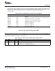
There are nine of these registers, one for each of nine logical blocks in the peripheral. The registers and
the blocks they support are listed in Table 46 . The general form for a block n enable register (BLK n_EN) is
shown in Figure 68 and described in Table 47 . For additional programming information, see
Section 2.3.10 .
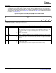
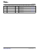
Table 46. Block n Enable Registers and the Associated Blocks
Register Address Offset Associated Block
BLK0_EN 0038h Logical block 0: the set of memory-mapped control registers for the SRIO
peripheral
BLK1_EN 0040h Logical block 1: the Load/Store module (the four LSUs and supporting logic)
BLK2_EN 0048h Logical block 2: the memory access unit (MAU)
BLK3_EN 0050h Logical block 3: the message transmit unit (TXU)
BLK4_EN 0058h Logical block 4: the message receive unit (RXU).
BLK5_EN 0060h Logical block 5: SRIO port 0
BLK6_EN 0068h Logical block 6: SRIO port 1.
BLK7_EN 0070h Logical block 7: SRIO port 2.
BLK8_EN 0078h Logical block 8: SRIO port 3.
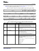
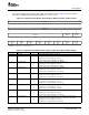
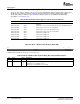
Figure 68. Block n Enable Register (BLK n_EN)
31 1 0
Reserved EN
R-0 R/W-1
LEGEND: R/W = Read/Write; R = Read only; - n = Value after reset
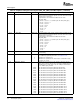
Table 47. Block n Enable Register (BLK n_EN) Field Descriptions
Bit Field Value Description
31-1 Reserved 0 Reserved
0 EN Block n enable
0 Logical block n is to be reset with its clock off.
1 Logical block n is to be enabled with its clock running.
SPRUE13A – September 2006 Serial RapidIO (SRIO) 119
Submit Documentation Feedback