
Stereo System - Digital Audio Signal Processor User Manual

SPRS079E – OCTOBER 1998 – REVISED AUGUST 2000
39
POST OFFICE BOX 1443 • HOUSTON, TEXAS 77251–1443
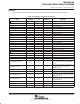
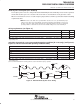
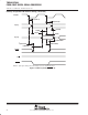
memory and parallel I/O interface timing
timing requirements for a
memory read (MSTRB = 0)
[H = 0.5 t
c(CO)
]
†
(see Figure 13)
MIN MAX UNIT
t
a(A)M
Access time, read data access from address valid 2H–7 ns
t
a(MSTRBL)
Access time, read data access from MSTRB low 2H–8 ns
t
su(D)R
Setup time, read data before CLKOUT low 6 ns
t
h(D)R
Hold time, read data after CLKOUT low –2 ns
t
h(A-D)R
Hold time, read data after address invalid 0 ns
t
h(D)MSTRBH
Hold time, read data after MSTRB high 0 ns
†
Address, PS, and DS timings are all included in timings referenced as address.
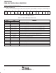
switching characteristics over recommended operating conditions for a
memory read
(MSTRB
= 0)
†
(see Figure 13)
PARAMETER MIN MAX UNIT
t
d(CLKL-A)
Delay time, CLKOUT low to address valid
‡
–2 3 ns
t
d(CLKH-A)
Delay time, CLKOUT high (transition) to address valid
§
–2 3 ns
t
d(CLKL-MSL)
Delay time, CLKOUT low to MSTRB low –1 3 ns
t
d(CLKL-MSH)
Delay time, CLKOUT low to MSTRB high –1 3 ns
t
h(CLKL-A)R
Hold time, address valid after CLKOUT low
‡
–2 3 ns
t
h(CLKH-A)R
Hold time, address valid after CLKOUT high
§
–2 3 ns
†
Address, PS, and DS timings are all included in timings referenced as address.
‡
In the case of a memory read preceded by a memory read
§
In the case of a memory read preceded by a memory write