
Car Stereo System User Manual

www.ti.com
Power Management
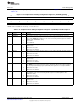
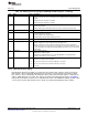
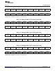
The peripheral clock gating configuration register 2 (PCGCR2) is shown in Figure 1-15 and described in
Table 1-25.
Figure 1-15. Peripheral Clock Gating Configuration Register 2 (PCGCR2) [1C03h]
15 8
Reserved
R-0
7 6 5 4 3 2 1 0
Reserved ANAREGCG DMA3CG DMA2CG DMA1CG USBCG SARCG LCDCG
R-0 R/W-0 R/W-0 R/W-0 R/W-0 R/W-0 R/W-0 R/W-0
LEGEND: R/W = Read/Write; R = Read only; -n = value after reset
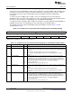
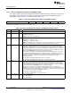
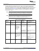
Table 1-25. Peripheral Clock Gating Configuration Register 2 (PCGCR2) Field Descriptions
Bit Field Value Description
15-7 Reserved 0 Reserved.
6 ANAREGCG Analog registers clock gate control bit. This bit is used to enable and disable the clock to the
registers that control the analog domain of the device, i.e. registers in the 7000h-70FFh I/O space
address range. NOTE When SARCG = 0, the clocks to the analog domain registers are enabled
regardless of the ANAREGCG setting.
0 Clock is active.
1 Clock is disabled.
5 DMA3CG DMA controller 3 clock gate control bit. This bit is used to enable and disable the DMA controller 3
peripheral clock.
0 Peripheral clock is active.
1 Peripheral clock is disabled.
4 DMA2CG DMA controller 2 clock gate control bit. This bit is used to enable and disable the DMA controller 2
peripheral clock.
0 Peripheral clock is active.
1 Peripheral clock is disabled.
3 DMA1CG DMA controller 1 clock gate control bit. This bit is used to enable and disable the DMA controller 1
peripheral clock.
0 Peripheral clock is active.
1 Peripheral clock is disabled.
2 USBCG USB clock gate control bit. This bit is used to enable and disable the USB controller peripheral
clock. NOTE You must request permission before stopping the USB clock through the peripheral
clock stop request/acknowledge register (CLKSTOP). This register does not stop the USB PLL.
0 Peripheral clock is active.
1 Peripheral clock is disabled.
1 SARCG SAR clock gate control bit. This bit is used to enable and disable the SAR peripheral clock. NOTE
When SARCG = 0, the clock to the analog domain registers is enabled regardless of the
ANAREGCG setting.
0 Peripheral clock is active.
1 Peripheral clock is disabled.
0 LCDCG LCD controller clock gate control bit. This bit is used to enable and disable the LCD controller
peripheral clock.
0 Peripheral clock is active.
1 Peripheral clock is disabled.
41
SPRUFX5A–October 2010–Revised November 2010 System Control
Submit Documentation Feedback
Copyright © 2010, Texas Instruments Incorporated