
Network Router User Manual

TMS380C26
NETWORK COMMPROCESSOR
SPWS010A–APRIL 1992–REVISED MARCH 1993
POST OFFICE BOX 1443 • HOUSTON, TEXAS
77251–1443
27
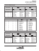
Bit 6: SWHRQ — Current SHRQ Signal Value
This bit contains the current value on the SHRQ/SBRQ pin when in Intel mode, and the inverse
of the SHRQ/SBRQ pin when in Motorola mode. This enables the host to easily determine if a
pseudo-DMA transfer is requested.
INTEL MODE (SI/M pin = H) MOTOROLA MODE (SI/M pin = L)
0 = System bus not requested System bus not requested
1 = System bus requested System bus requested
Bit 7: PSDMAEN — Pseudo-System-DMA Enable
This bit enables pseudo-DMA operation
0 = Normal bus master DMA operation possible.
1 = Pseudo-DMA operation selected. Operation dependent on the values of the SWHLDA
and SWHRQ bits in the SIFACL register.
Bit 8: ARESET — Adapter Reset
This bit is a hardware reset of the TMS380C26. This bit has the same effect as the SRESET pin,
except that the DIO interface to the SIFACL register is maintained. This bit will be set to one if
a clock failure is detected (OSCIN, PXTALIN, RCLK, or SBCLK not valid).
0 = The TMS380C26 operates normally.
1 = The TMS380C26 is held in the reset condition.
Bit 9: CPHALT — Communications Processor Halt
This bit prevents the TMS380C26’s processor from accessing the internal TMS380C26 buses.
This prevents the TMS380C26 from executing instructions before the microcode has been
downloaded.
0 = The TMS380C26’s processor can access the internal TMS380C26 buses.
1 = The TMS380C26’s processor is prevented from accessing the internal adapter buses.
Bit 10: BOOT — Bootstrap CP Code
This bit indicates whether the memory in chapters 0 and 31 of the local memory space is RAM
or ROM/PROM/EPROM. This bit then controls the operation of the MCAS
and MROMEN pins.
0 = ROM/PROM/EPROM memory in chapters 0 and 31.
1 = RAM memory in chapters 0 and 31.
Bit 11: RES0 — Reserved. This bit must be set to zero