
Network Router User Manual

TMS380C26
NETWORK COMMPROCESSOR
SPWS010A–APRIL 1992–REVISED MARCH 1993
POST OFFICE BOX 1443 • HOUSTON, TEXAS
77251–1443
34
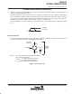
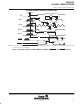
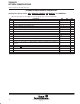
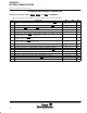
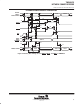
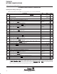
PARAMETER MEASUREMENT INFORMATION
power up, SBCLK, OSCIN, MBCLK1, MBCLK2, SYNCIN
, and SRESET timing
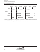
NO. PARAMETER MIN MAX UNIT
100
†
t
r(VDD
) Rise time from 1.2 V to V
DD
minimum high level 1 ms
101
†‡
t
d(VDDH-SCKV)
Delay time from minimum V
DD
high level to first valid SBCLK no longer high 1 ms
102
†‡
t
d(VDDH-OSCV)
Delay time from minimum V
DD
high level to first valid OSCIN high 1 ms
103 t
c(SCK)
Cycle time of SBCLK 62.5 ns
104 t
w(SCKH)
Pulse duration of SBCLK high 26 ns
105 t
w(SCKL)
Pulse duration of SBCLK low 26 ns
106
†
t
t(SCK)
Transition time of SBCLK 5 ns
107 t
c(OSC)
Cycle time of OSCIN (see Note 12) 15.6 500 ns
108 t
w(OSCH)
Pulse duration of OSCIN high 5.5 ns
109 t
w(OSCL)
Pulse duration of OSCIN low 5.5 ns
110
†
t
t(OSC)
Transition time of OSCIN 3 ns
111
†
t
d(OSCV-CKV)
Delay time from OSCIN valid to MBCLK1 and MBCLK2 valid 1 ms
117
†
t
h(VDDH-RSL)
Hold time of SRESET low after V
DD
reaches minimum high level 5 ms
118
†
t
w(RSH)
Pulse duration of SRESET high 14 µs
119
†
t
w(RSL)
Pulse duration of SRESET low 14 µs
288
†
t
su(RST)
Setup time of DMA size to SRESET high (Intel mode only) 15 ns
289
†
t
h(RST)
Hold time of DMA size from SRESET high (Intel mode only) 15 ns
t
M
One-eighth of an local memory cycle 2t
c(OSC)
†
This specification is provided as an aid to board design.
‡
If parameter 101 or 102 cannot be met, parameter 117 must be extended by the larger difference: real value of parameter 101 or 102 minus the
max value listed.
NOTE 12: If OSCIN is used to generate PXTALIN, the specification for the tolerance of OSCIN is equal to ± 0.01%.