
Network Router User Manual


TMS380C26
NETWORK COMMPROCESSOR
SPWS010A–APRIL 1992–REVISED MARCH 1993
POST OFFICE BOX 1443 • HOUSTON, TEXAS
77251–1443
79
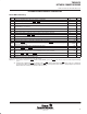
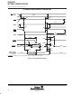
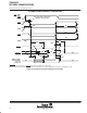
PARAMETER MEASUREMENT INFORMATION
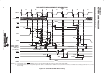
68xxx interrupt acknowledge cycle timing
NO. PARAMETER MIN MAX UNIT
255 Delay from SDTACK low to either SCS or SUDS, or SIACK high 15 ns
259
†
Hold of SAD high-impedance after SIACK no longer high (see Note 21) 0 ns
260 Setup of output data valid before SDTACK no longer high 0 ns
261
†
Delay from SIACK high to SAD high-impedance (see Note 21) 35 ns
261a Hold of output data valid after SCS or SIACK no longer low (see Note 21) 0 ns
267
§
Setup of register address before SIACK no longer high (see Note 21) 15 ns
272a Setup of inactive high SIACK to active data strobe no longer high 55 ns
273a Hold of inactive SRNW high after active data strobe high 55 ns
275 Delay from SCS or SRNW high to SDTACK high (see Note 21) 35 ns
276
‡
Delay from SDTACK low in the first DIO access to the SIF register to SDTACK low in the immediately
following access to the SIF
4000 ns
279
†
Delay from SIACK high to SDTACK high impedance 65 ns
282a Delay from SDBEN low to SDTACK low in a read cycle 35 ns
282R
Delay from SIACK low to SDBEN low (see
TMS380 Second Generation Token-Ring User’s Guide,
SPWU005
,
subsection 3.4.1.1.1) provided the previous cycle completed
55 ns
283R Delay from SIACK high to SDBEN high (see Note 21) 35 ns
286 Pulse duration, SIACK high between DIO accesses (see Note 21) 55 ns
†
This specification is provided as an aid to board design.
‡
This specification has been characterized to meet stated value.
§
It is the later of SRD
and SRD or SCS low that indicates the start of the cycle.
NOTE 21: The “inactive” chip select is SIACK
in DIO read and DIO write cycles, and SCS is the “inactive” chip select in interrupt acknowledge
cycles.