TMS470R1B1M 16/32-Bit RISC Flash Microcontroller www.ti.
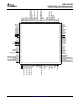
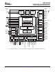
TMS470R1B1M 16/32-Bit RISC Flash Microcontroller www.ti.com SPNS109A – SEPTEMBER 2005 – REVISED AUGUST 2006 • 144-Pin Plastic Low-Profile Quad Flatpack (PGE Suffix) (1) The test-access port is compatible with the IEEE Standard 1149.1-1990, IEEE Standard Test-Access Port and Boundary Scan Architecture specification. Boundary scan is not supported on this device.
TMS470R1B1M 16/32-Bit RISC Flash Microcontroller www.ti.
TMS470R1B1M 16/32-Bit RISC Flash Microcontroller www.ti.com SPNS109A – SEPTEMBER 2005 – REVISED AUGUST 2006 DESCRIPTION The TMS470R1B1M (1) devices are members of the Texas Instruments TMS470R1x family of general-purpose 16/32-bit reduced instruction set computer (RISC) microcontrollers. The B1M microcontroller offers high performance utilizing the high-speed ARM7TDMI 16/32-bit RISC central processing unit (CPU), resulting in a high instruction throughput while maintaining greater code efficiency.
TMS470R1B1M 16/32-Bit RISC Flash Microcontroller www.ti.com SPNS109A – SEPTEMBER 2005 – REVISED AUGUST 2006 The flash memory on this device is a nonvolatile, electrically erasable and programmable memory implemented with a 32-bit-wide data bus interface. The flash operates with a system clock frequency of up to 24 MHz or 30 MHz, depending on the input voltage. When in pipeline mode, the flash operates with a system clock frequency of up to 48 MHz or 60 MHz, depending on the input voltage.
TMS470R1B1M 16/32-Bit RISC Flash Microcontroller www.ti.com SPNS109A – SEPTEMBER 2005 – REVISED AUGUST 2006 The B1M device also has an external clock prescaler (ECP) module that when enabled, outputs a continuous external clock (ECLK) on a specified GIO pin. The ECLK frequency is a user-programmable ratio of the peripheral interface clock (ICLK) frequency. For more detailed functional information on the ECP, see the TMS470R1x External Clock Prescaler (ECP) Reference Guide (literature number SPNU202).
TMS470R1B1M 16/32-Bit RISC Flash Microcontroller www.ti.
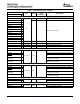
TMS470R1B1M 16/32-Bit RISC Flash Microcontroller www.ti.com SPNS109A – SEPTEMBER 2005 – REVISED AUGUST 2006 Table 2. Terminal Functions TERMINAL NAME NO. TYPE (1) (2) CURRENT OUTPUT INTERNAL PULLUP/ PULLDOWN (3) DESCRIPTION HIGH-END TIMER (HET) HET[0] 73 HET[1] 72 HET[2] 71 HET[3] 66 HET[4] 65 HET[5] 63 HET[6] 9 HET[7] 11 HET[8] 12 HET[18] 15 HET[20] 18 HET[22] 19 CAN1HRX 83 CAN1HTX CAN2HRX CAN2HTX 3.3 V 2 mA -z IPD (20 µA) Timer input capture or output compare.
TMS470R1B1M 16/32-Bit RISC Flash Microcontroller www.ti.com SPNS109A – SEPTEMBER 2005 – REVISED AUGUST 2006 Table 2. Terminal Functions (continued) TERMINAL NAME NO.
TMS470R1B1M 16/32-Bit RISC Flash Microcontroller www.ti.com SPNS109A – SEPTEMBER 2005 – REVISED AUGUST 2006 Table 2. Terminal Functions (continued) TERMINAL NAME NO. CURRENT OUTPUT TYPE (1) (2) INTERNAL PULLUP/ PULLDOWN (3) DESCRIPTION MULTI-BUFFERED ANALOG-TO-DIGITAL CONVERTER (MibADC) 2 mA -z IPD (20 µA) MibADC event input. Can be programmed as a GIO pin.
TMS470R1B1M 16/32-Bit RISC Flash Microcontroller www.ti.com SPNS109A – SEPTEMBER 2005 – REVISED AUGUST 2006 Table 2. Terminal Functions (continued) TERMINAL NAME NO.
TMS470R1B1M 16/32-Bit RISC Flash Microcontroller www.ti.com SPNS109A – SEPTEMBER 2005 – REVISED AUGUST 2006 Table 2. Terminal Functions (continued) TERMINAL NAME NO. TYPE (1) (2) CURRENT OUTPUT INTERNAL PULLUP/ PULLDOWN (3) DESCRIPTION WATCHDOG/REAL-TIME INTERRUPT (WD/RTI) AWD 36 TCK 76 TDI 74 TDO 75 TEST 124 TMS 17 TMS2 16 TRST 144 3.3 V Analog watchdog reset.
TMS470R1B1M 16/32-Bit RISC Flash Microcontroller www.ti.com SPNS109A – SEPTEMBER 2005 – REVISED AUGUST 2006 Table 2. Terminal Functions (continued) TERMINAL NAME NO.
TMS470R1B1M 16/32-Bit RISC Flash Microcontroller www.ti.com SPNS109A – SEPTEMBER 2005 – REVISED AUGUST 2006 B1M Device-Specific Information Memory Figure 1 shows the memory map of the B1M device.
TMS470R1B1M 16/32-Bit RISC Flash Microcontroller www.ti.com SPNS109A – SEPTEMBER 2005 – REVISED AUGUST 2006 memory selects Memory selects allow the user to address memory arrays (i.e., flash, RAM, and HET RAM) at user-defined addresses. Each memory select has its own set (low and high) of memory base address registers (MFBAHRx and MFBALRx) that, together, define the array's starting (base) address, block size, and protection.
TMS470R1B1M 16/32-Bit RISC Flash Microcontroller www.ti.com SPNS109A – SEPTEMBER 2005 – REVISED AUGUST 2006 flash protection keys The B1M device provides flash protection keys. These four 32-bit protection keys prevent program/erase/compaction operations from occurring until after the four protection keys have been matched by the CPU loading the correct user keys into the FMPKEY control register. The protection keys on the B1M are located in the last 4 words of the first 64K sector.
TMS470R1B1M 16/32-Bit RISC Flash Microcontroller www.ti.com SPNS109A – SEPTEMBER 2005 – REVISED AUGUST 2006 flash program and erase The B1M device flash contains two 512K-byte memory arrays (or banks), for a total of 1M-byte of flash, and consists of sixteen sectors. These sixteen sectors are sized as follows: SECTOR NO.
TMS470R1B1M 16/32-Bit RISC Flash Microcontroller www.ti.com SPNS109A – SEPTEMBER 2005 – REVISED AUGUST 2006 peripheral selects and base addresses The B1M device uses 10 of the 16 peripheral selects to decode the base addresses of the peripherals. These peripheral selects are fixed and transparent to the user since they are part of the decoding scheme used by the SYS module. Control registers for the peripherals, SYS module, and flash begin at the base addresses shown in Table 4. Table 4.
TMS470R1B1M 16/32-Bit RISC Flash Microcontroller www.ti.com SPNS109A – SEPTEMBER 2005 – REVISED AUGUST 2006 Table 4.
TMS470R1B1M 16/32-Bit RISC Flash Microcontroller www.ti.com SPNS109A – SEPTEMBER 2005 – REVISED AUGUST 2006 direct-memory access (DMA) The direct-memory access (DMA) controller transfers data to and from any specified location in the B1M memory map (except for restricted memory locations like the system control registers area). The DMA manages up to 16 channels, and supports data transfer for both on-chip and off-chip memories and peripherals.
TMS470R1B1M 16/32-Bit RISC Flash Microcontroller www.ti.com SPNS109A – SEPTEMBER 2005 – REVISED AUGUST 2006 interrupt priority (IEM to CIM) Interrupt requests originating from the B1M peripheral modules (i.e., SPI1 or SPI2; SCI1 or SCI2; RTI; etc.) are assigned to channels within the 48-channel interrupt expansion module (IEM) where, via programmable register mapping, these channels are then mapped to the 32-channel central interrupt manager (CIM) portion of the SYS module.
TMS470R1B1M 16/32-Bit RISC Flash Microcontroller www.ti.com SPNS109A – SEPTEMBER 2005 – REVISED AUGUST 2006 Table 6.
TMS470R1B1M 16/32-Bit RISC Flash Microcontroller www.ti.com SPNS109A – SEPTEMBER 2005 – REVISED AUGUST 2006 expansion bus module (EBM) The expansion bus module (EBM) is a standalone module used to bond out both general-purpose input/output pins and expansion bus interface pins. This module supports the multiplexing of the GIO and the expansion bus interface functions.
TMS470R1B1M 16/32-Bit RISC Flash Microcontroller www.ti.com SPNS109A – SEPTEMBER 2005 – REVISED AUGUST 2006 MibADC The multi-buffered analog-to-digital converter (MibADC) accepts an analog signal and converts the signal to a 10-bit digital value.
TMS470R1B1M 16/32-Bit RISC Flash Microcontroller www.ti.com SPNS109A – SEPTEMBER 2005 – REVISED AUGUST 2006 JTAG Interface There are two main test access ports (TAPs) on the device: • TMS470R1x CPU TAP • Device TAP for factory test Some of the JTAG pins are shared among these two TAPs. The hookup is illustrated in Figure 2. TMS470R1x CPU TCK TCK TRST TRST TMS TMS TDI TDI TDO TDO Factory Test TCK TRST TMS2 TMS TDI TDO Figure 2.
TMS470R1B1M 16/32-Bit RISC Flash Microcontroller www.ti.com SPNS109A – SEPTEMBER 2005 – REVISED AUGUST 2006 documentation support Extensive documentation supports all of the TMS470 microcontroller family generation of devices. The types of documentation available include data sheets with design specifications; complete user's guides for all devices and development support tools; and hardware and software applications.
TMS470R1B1M 16/32-Bit RISC Flash Microcontroller www.ti.com SPNS109A – SEPTEMBER 2005 – REVISED AUGUST 2006 Device and Development-Support Tool Nomenclature To designate the stages in the product development cycle, TI assigns prefixes to the part numbers of all DSP devices and support tools. Each DSP commercial family member has one of three prefixes: TMX, TMP, or TMS (e.g., TMS470R1B1M). Texas Instruments recommends two of three possible prefix designators for its support tools: TMDX and TMDS.
TMS470R1B1M 16/32-Bit RISC Flash Microcontroller www.ti.com SPNS109A – SEPTEMBER 2005 – REVISED AUGUST 2006 TMS 470 R1 B 1M PGE A OPTIONS PREFIX TMS = Fully Qualified Device FAMILY 470 = TMS470 RISC − Embedded Microcontroller Family TEMPERATURE RANGE A = −40°C − 85 °C PACKAGE TYPE PGE = 144-pin Low-Profile Quad Flatpack (LQFP) ARCHITECTURE R1 = ARM7TDM1 CPU DEVICE TYPE B With 1024K−Bytes Flash Memory: 60−MHZ Frequency 1.8-V Core, 3.
TMS470R1B1M 16/32-Bit RISC Flash Microcontroller www.ti.com SPNS109A – SEPTEMBER 2005 – REVISED AUGUST 2006 device identification code register The device identification code register identifies the silicon version, the technology family (TF), a ROM or flash device, and an assigned device-specific part number (see Table 10). The B1M device identification code register value is 0xnA5F. Figure 4.
TMS470R1B1M 16/32-Bit RISC Flash Microcontroller www.ti.com SPNS109A – SEPTEMBER 2005 – REVISED AUGUST 2006 DEVICE ELECTRICAL SPECIFICATIONS AND TIMING PARAMETERS Absolute Maximum Ratings over operating free-air temperature range, A version (unless otherwise noted) (1) Supply voltage range: VCC (2) –0.3 V to 2.5 V (2) Supply voltage range: VCCIO, VCCAD, VCCP (flash pump) Input voltage range: All 5 V tolerant input pins – 0.3 V to 6.0 V All other input pins –0.3 V to 4.
TMS470R1B1M 16/32-Bit RISC Flash Microcontroller www.ti.com SPNS109A – SEPTEMBER 2005 – REVISED AUGUST 2006 ELECTRICAL CHARACTERISTICS over recommended operating free-air temperature range (1) PARAMETER Vhys Input hysteresis VIL Low-level input voltage All inputs (3) VIH High-level input voltage All inputs VIH Input threshold voltage AWD only (4) VOL Low-level output voltage (5) VOH High-level output voltage (5) IIC Input clamp current (I/O pins) (6) Input current (3.
TMS470R1B1M 16/32-Bit RISC Flash Microcontroller www.ti.com SPNS109A – SEPTEMBER 2005 – REVISED AUGUST 2006 ELECTRICAL CHARACTERISTICS (continued) over recommended operating free-air temperature range PARAMETER ICCIO TEST CONDITIONS MAX UNIT VCCIO Digital supply current (operating mode) No DC load, VCCIO = 3.6 15 mA VCCIO Digital supply current (standby mode) (9) No DC load, VCCIO = 3.6 V (10) 10 µA VCCIO Digital supply current (halt mode) (9) No DC load, VCCIO = 3.
TMS470R1B1M 16/32-Bit RISC Flash Microcontroller www.ti.com SPNS109A – SEPTEMBER 2005 – REVISED AUGUST 2006 Timing Parameter Symbology Timing parameter symbols have been created in accordance with JEDEC Standard 100.
TMS470R1B1M 16/32-Bit RISC Flash Microcontroller www.ti.com SPNS109A – SEPTEMBER 2005 – REVISED AUGUST 2006 External Reference Resonator/Crystal Oscillator Clock Option The oscillator is enabled by connecting the appropriate fundamental 4–10 MHz resonator/crystal and load capacitors across the external OSCIN and OSCOUT pins as shown in Figure 6a. The oscillator is a single-stage inverter held in bias by an integrated bias resistor. This resistor is disabled during leakage test measurement and HALT mode.
TMS470R1B1M 16/32-Bit RISC Flash Microcontroller www.ti.
TMS470R1B1M 16/32-Bit RISC Flash Microcontroller www.ti.com SPNS109A – SEPTEMBER 2005 – REVISED AUGUST 2006 Switching Characteristics over Recommended Operating Conditions for External Clocks (1) (2) (3) (see Figure 7 and Figure 8) PARAMETER TEST CONDITIONS MIN SYSCLK or MCLK (4) tw(COL) ICLK: X is even or 1 (5) Pulse duration, CLKOUT low ICLK: X is odd and not tw(COH) Pulse duration, CLKOUT high tw(EOL) tw(EOH) Pulse duration, ECLK low Pulse duration, ECLK high 0.5tc(ICLK) – tf 1 (5) 0.
TMS470R1B1M 16/32-Bit RISC Flash Microcontroller www.ti.
TMS470R1B1M 16/32-Bit RISC Flash Microcontroller www.ti.
TMS470R1B1M 16/32-Bit RISC Flash Microcontroller www.ti.
TMS470R1B1M 16/32-Bit RISC Flash Microcontroller www.ti.com SPNS109A – SEPTEMBER 2005 – REVISED AUGUST 2006 INPUT TIMINGS Timing Requirements for Input Timings (1) (see Figure 12) MIN tpw (1) Input minimum pulse width MAX UNIT tc(ICLK) + 10 ns tc(ICLK) = interface clock cycle time = 1/f(ICLK) tpw Input 80% V CC 80% 20% 20% 0 Figure 12.
TMS470R1B1M 16/32-Bit RISC Flash Microcontroller www.ti.com SPNS109A – SEPTEMBER 2005 – REVISED AUGUST 2006 SPIn MASTER MODE TIMING PARAMETERS SPIn Master Mode External Timing Parameters (CLOCK PHASE = 0, SPInCLK = output, SPInSIMO = output, and SPInSOMI = input) (1) (2) (3) (see Figure 13) NO. 1 2 (5) 3 (5) 4 (5) 5 (5) 6 (5) 7 (5) (1) (2) (3) (4) (5) MIN MAX 100 256tc(ICLK) Pulse duration, SPInCLK high (clock polarity = 0) 0.5tc(SPC)M – tr 0.
TMS470R1B1M 16/32-Bit RISC Flash Microcontroller www.ti.com SPNS109A – SEPTEMBER 2005 – REVISED AUGUST 2006 SPIn Master Mode External Timing Parameters (CLOCK PHASE = 1, SPInCLK = output, SPInSIMO = output, and SPInSOMI = input) (1) (2) (3) (see Figure 14) NO. 1 2 (5) 3 (5) MIN MAX 100 256tc(ICLK) Pulse duration, SPInCLK high (clock polarity = 0) 0.5tc(SPC)M – tr 0.5tc(SPC)M + 5 tw(SPCL)M Pulse duration, SPInCLK low (clock polarity = 1) 0.5tc(SPC)M – tf 0.
TMS470R1B1M 16/32-Bit RISC Flash Microcontroller www.ti.com SPNS109A – SEPTEMBER 2005 – REVISED AUGUST 2006 SPIn SLAVE MODE TIMING PARAMETERS SPIn Slave Mode External Timing Parameters (CLOCK PHASE = 0, SPInCLK = input, SPInSIMO = input, and SPInSOMI = output) (1) (2) (3) (4) (see Figure 15) NO. 1 2 (6) 3 (6) MIN tc(SPC)S Cycle time, SPInCLK (5) 100 256tc(ICLK) tw(SPCH)S Pulse duration, SPInCLK high (clock polarity = 0) 0.5tc(SPC)S – 0.25tc(ICLK) 0.5tc(SPC)S + 0.
TMS470R1B1M 16/32-Bit RISC Flash Microcontroller www.ti.com SPNS109A – SEPTEMBER 2005 – REVISED AUGUST 2006 1 SPInCLK (clock polarity = 0) 2 3 SPInCLK (clock polarity = 1) 4 55 SPInSOMI SPISOMI Data Is Valid 6 7 SPInSIMO SPISIMO Data Must Be Valid Figure 15.
TMS470R1B1M 16/32-Bit RISC Flash Microcontroller www.ti.com SPNS109A – SEPTEMBER 2005 – REVISED AUGUST 2006 SPIn Slave Mode External Timing Parameters (CLOCK PHASE = 1, SPInCLK = input, SPInSIMO = input, and SPInSOMI = output) (1) (2) (3) (4) (see Figure 16) NO. 1 2 (6) 3 (6) 100 256tc(ICLK) Cycle time, SPInCLK (5) tw(SPCH)S Pulse duration, SPInCLK high (clock polarity = 0) 0.5tc(SPC)S – 0.25tc(ICLK) 0.5tc(SPC)S + 0.25tc(ICLK) tw(SPCL)S Pulse duration, SPInCLK low (clock polarity = 1) 0.
TMS470R1B1M 16/32-Bit RISC Flash Microcontroller www.ti.com SPNS109A – SEPTEMBER 2005 – REVISED AUGUST 2006 SCIn ISOSYNCHRONOUS MODE TIMINGS - INTERNAL CLOCK Timing Requirements for Internal Clock SCIn Isosynchronous Mode (1) (2) (3) (see Figure 17) (BAUD + 1) IS EVEN OR BAUD = 0 (BAUD + 1) IS ODD AND BAUD ≠ 0 UNIT MIN MAX MIN MAX 2tc(ICLK) 224 tc(ICLK) 3tc(ICLK) (224 – 1) tc(ICLK) ns tc(SCC) Cycle time, SCInCLK tw(SCCL) Pulse duration, SCInCLK low 0.5tc(SCC) – tf 0.5tc(SCC) + 5 0.
TMS470R1B1M 16/32-Bit RISC Flash Microcontroller www.ti.com SPNS109A – SEPTEMBER 2005 – REVISED AUGUST 2006 SCIn ISOSYNCHRONOUS MODE TIMINGS - EXTERNAL CLOCK Timing Requirements for External Clock SCIn Isosynchronous Mode (1) (2) (see Figure 18) MIN MAX UNIT tc(SCC) Cycle time, SCInCLK (3) tw(SCCH) Pulse duration, SCInCLK high 0.5tc(SCC) – 0.25tc(ICLK) 0.5tc(SCC) + 0.25tc(ICLK) ns tw(SCCL) Pulse duration, SCInCLK low 0.5tc(SCC) – 0.25tc(ICLK) 0.5tc(SCC) + 0.
TMS470R1B1M 16/32-Bit RISC Flash Microcontroller www.ti.com SPNS109A – SEPTEMBER 2005 – REVISED AUGUST 2006 I2C TIMING Table 11 assumes testing over recommended operating conditions. I2C Signals (SDA and SCL) Switching Characteristics (1) STANDARD MODE PARAMETER MIN MAX 150 FAST MODE MIN MAX 75 150 UNIT tc(I2CCLK) Cycle time, I2C module clock 75 tc(SCL) Cycle time, SCL 10 2.5 µs tsu(SCLH-SDAL) Setup time, SCL high before SDA low (for a repeated START condition) 4.7 0.
TMS470R1B1M 16/32-Bit RISC Flash Microcontroller www.ti.com SPNS109A – SEPTEMBER 2005 – REVISED AUGUST 2006 STANDARD CAN CONTROLLER (SCC) MODE TIMINGS Dynamic Characteristics for the CANSTX and CANSRX Pins PARAMETER MIN pin (1) td(CANSTX) Delay time, transmit shift register to CANSTX td(CANSRX) Delay time, CANSRX pin to receive shift register (1) MAX UNIT 15 ns 5 ns These values do not include the rise/fall times of the output buffer.
TMS470R1B1M 16/32-Bit RISC Flash Microcontroller www.ti.com SPNS109A – SEPTEMBER 2005 – REVISED AUGUST 2006 EXPANSION BUS MODULE TIMING Expansion Bus Timing Parameters –40°C ≤ TJ≤ 150°C, 3.0 V ≤ V CC≤ 3.6 V (see Figure 20 and Figure 21) MIN MAX 20.8 UNIT tc(CO) Cycle time, CLKOUT td(COH-EBADV) Delay time, CLKOUT high to EBADDR valid 21.4 ns ns th(COH-EBADIV) Hold time, EBADDR invalid after CLKOUT high 12.4 ns td(COH-EBOE) Delay time, CLKOUT high to EBOE fall 11.
TMS470R1B1M 16/32-Bit RISC Flash Microcontroller www.ti.com SPNS109A – SEPTEMBER 2005 – REVISED AUGUST 2006 tc(CO) CLKOUT th(COH-EBADIV) td(COH-EBADV) Valid EBADDR th(COL-EBWDATIV) td(COL-EBWDATV) Valid EBDATA th(COL-EBWRH) td(COL-EBWR) EBWR td(COH-EBCS0) td(COH-EBCS0) EBCS0 tsu(COH-EBHOLDH) tsu(COH-EBHOLDL) EBHOLD 1 Hold State Figure 21.
TMS470R1B1M 16/32-Bit RISC Flash Microcontroller www.ti.com SPNS109A – SEPTEMBER 2005 – REVISED AUGUST 2006 HIGH-END TIMER (HET) TIMINGS Minimum PWM Output Pulse Width: This is equal to one high resolution clock period (HRP). The HRP is defined by the 6-bit high resolution prescale factor (hr), which is user defined, giving prescale factors of 1 to 64, with a linear increment of codes.
TMS470R1B1M 16/32-Bit RISC Flash Microcontroller www.ti.com SPNS109A – SEPTEMBER 2005 – REVISED AUGUST 2006 MULTI-BUFFERED A-TO-D CONVERTER (MibADC) The multi-buffered A-to-D converter (MibADC) has a separate power bus for its analog circuitry that enhances the A-to-D performance by preventing digital switching noise on the logic circuitry, which could be present on V SS and V CC , from coupling into the A-to-D analog stage.
TMS470R1B1M 16/32-Bit RISC Flash Microcontroller www.ti.com SPNS109A – SEPTEMBER 2005 – REVISED AUGUST 2006 External Rs MibADC Input Pin Ri Sample Switch Sample Capacitor Parasitic Capacitance V src R leak Ci Figure 22. MibADC Input Equivalent Circuit Table 19. Multi-Buffer ADC Timing Requirements MIN tc(ADCLK) Cycle time, MibADC clock td(SH) Delay time, sample and hold time td©) td(SHC) (1) (1) NOM MAX UNIT 0.05 µs 1 µs Delay time, conversion time 0.
TMS470R1B1M 16/32-Bit RISC Flash Microcontroller www.ti.com SPNS109A – SEPTEMBER 2005 – REVISED AUGUST 2006 The integral nonlinearity error shown in Figure 24 (sometimes referred to as linearity error) is the deviation of the values on the actual transfer function from a straight line. 0 ... 111 0 ... 110 Ideal Transition 0 ... 101 Actual Transition 0 ... 100 At Transition 011/100 (ć 1/2 LSB) 0 ... 011 0 ... 010 End-Point Lin. Error 0 ... 001 At Transition 001/010 (ć 1/4 LSB) 0 ...
TMS470R1B1M 16/32-Bit RISC Flash Microcontroller www.ti.
TMS470R1B1M 16/32-Bit RISC Flash Microcontroller www.ti.com SPNS109A – SEPTEMBER 2005 – REVISED AUGUST 2006 Revision History This revision history highlights the changes made to the device-specific datasheet SPNS109. Table 12. Revision History SPNS109 to SPNS109A Added note to PORRST Timing Diagram. Changed TA range to –40°C to 85°C on twec in "Timing Requirements for Program Flash" table. Changed twec MIN value to 50000 and deleted TYP value in "Timing Requirements for Program Flash" table.
PACKAGE OPTION ADDENDUM www.ti.
MECHANICAL DATA MTQF017A – OCTOBER 1994 – REVISED DECEMBER 1996 PGE (S-PQFP-G144) PLASTIC QUAD FLATPACK 108 73 109 72 0,27 0,17 0,08 M 0,50 144 0,13 NOM 37 1 36 Gage Plane 17,50 TYP 20,20 SQ 19,80 22,20 SQ 21,80 0,25 0,05 MIN 0°– 7° 0,75 0,45 1,45 1,35 Seating Plane 0,08 1,60 MAX 4040147 / C 10/96 NOTES: A. All linear dimensions are in millimeters. B. This drawing is subject to change without notice. C.
IMPORTANT NOTICE Texas Instruments Incorporated and its subsidiaries (TI) reserve the right to make corrections, modifications, enhancements, improvements, and other changes to its products and services at any time and to discontinue any product or service without notice. Customers should obtain the latest relevant information before placing orders and should verify that such information is current and complete.