TP3064, TP3067 Enhanced Serial Interface CMOS CODEC/Filter COMBO Literature Number: SNAS570
TP3064, TP3067 ‘‘Enhanced’’ Serial Interface CMOS CODEC/Filter COMBOÉ General Description Features The TP3064 (m-law) and TP3067 (A-law) are monolithic PCM CODEC/Filters utilizing the A/D and D/A conversion architecture shown in Figure 1 , and a serial PCM interface. The devices are fabricated using National’s advanced double-poly CMOS process (microCMOS). Similar to the TP305X family, these devices feature an additional Receive Power Amplifier to provide push-pull balanced output drive capability.
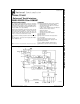
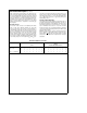
Connection Diagrams Plastic Chip Carrier Dual-In-Line Package TL/H/5070 – 6 Top View Order Number TP3064J or TP3067J See NS Package J20A Order Number TP3064WM or TP3067WM See NS Package M20B Order Number TP3064N or TP3067N See NS Package N20A TL/H/5070–2 Top View Order Number TP3064V or TP3067V See NS Package V20A Pin Description Symbol VPO a GNDA VPOb VPI VFRO VCC FSR DR BCLKR/ CLKSEL MCLKR/ PDN Symbol MCLKX Function The non-inverted output of the receive power amplifier. Analog ground.
Functional Description sion performance, however, MCLKR should be synchronous with MCLKX, which is easily achieved by applying only static logic levels to the MCLKR/PDN pin. This will automatically connect MCLKX to all internal MCLKR functions (see Pin Description). For 1.544 MHz operation, the device automatically compensates for the 193rd clock pulse each frame. FSX starts each encoding cycle and must be synchronous with MCLKX and BCLKX. FSR starts each decoding cycle and must be synchronous with BCLKR.
Functional Description (Continued) table of Transmission Characteristics). The FSX frame sync pulse controls the sampling of the filter output, and then the successive-approximation encoding cycle begins. The 8-bit code is then loaded into a buffer and shifted out through DX at the next FSX pulse. The total encoding delay will be approximately 165 ms (due to the transmit filter) plus 125 ms (due to encoding delay), which totals 290 ms.
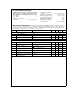
Absolute Maximum Ratings Voltage at any Digital Input or Output If Military/Aerospace specified devices are required, please contact the National Semiconductor Sales Office/Distributors for availability and specifications. VCC to GNDA VBB to GNDA Voltage at any Analog Input or Output VCC a 0.3V to GNDAb0.3V Operating Temperature Range Storage Temperature Range Lead Temp. (Soldering, 10 sec.) ESD (Human Body Model) J ESD (Human Body Model) N Latch-Up Immunity 7V b 7V VCC a 0.3V to VBBb0.
Electrical Characteristics (Continued) Unless otherwise noted, limits printed in BOLD characters are guaranteed for VCC e a 5.0V g 5%, VBB e b5.0V g 5%; TA e 0§ C to 70§ C by correlation with 100% electrical testing at TA e 25§ C. All other limits are assured by correlation with other production tests and/or product design and characterization. All signals referenced to GNDA. Typicals specified at VCC e a 5.0V, VBB e b 5.0V, TA e 25§ C.
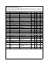
Timing Specifications Unless otherwise noted, limits printed in BOLD characters are guaranteed for VCC e a 5.0V g 5%, VBB e b5.0V g 5%, TA e 0§ C to 70§ C by correlation with 100% electrical testing at TA e 25§ C. All other limits are assured by correlation with other production tests and/or product design and characterization. All signals are referenced to GNDA. Typicals specified at VCC e a 5.0V, VBB e b 5.0V, TA e 25§ C. All timing parameters are measured at VOH e 2.0V and VOL e 0.7V.
FIGURE 2.
FIGURE 3.
Transmission Characteristics Unless otherwise noted, limits printed in BOLD characters are guaranteed for VCC e a 5.0V g 5%, VBB e b5.0V g 5%; TA e 0§ C to 70§ C by correlation with 100% electrical testing at TA e 25§ C. All other limits are assured by correlation with other production tests and/or product design and characterization. GNDA e 0V, f e 1.02 kHz, VIN e 0 dbm0, transmit input amplifier connected for unity gain non-inverting. Typicals specified at VCC e a 5.0V, VBB e b5.0V, TA e 25§ C.
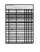
Transmission Characteristics (Continued) Unless otherwise noted, limits printed in BOLD characters are guaranteed for VCC e a 5.0V g 5%, VBB e b5.0V g 5%; TA e 0§ C to 70§ C by correlation with 100% electrical testing at TA e 25§ C. All other limits are assured by correlation with other production tests and/or product design and characterization. GNDA e 0V, f e 1.02 kHz, VIN e 0 dbm0, transmit input amplifier connected for unity gain non-inverting. Typicals specified at VCC e a 5.0V, VBB e b5.
Transmission Characteristics (Continued) Unless otherwise noted, limits printed in BOLD characters are guaranteed for VCC e a 5.0V g 5%, VBB e b5.0V g 5%; TA e 0§ C to 70§ C by correlation with 100% electrical testing at TA e 25§ C. All other limits are assured by correlation with other production tests and/or product design and characterization. GNDA e 0V, f e 1.02 kHz, VIN e 0 dbm0, transmit input amplifier connected for unity gain non-inverting. Typicals specified at VCC e a 5.0V, VBB e b5.
Applications Information POWER SUPPLIES While the pins of the TP3060 family are well protected against electrical misuse, it is recommended that the standard CMOS practice be followed, ensuring that ground is connected to the device before any other connections are made. In applications where the printed circuit board may be plugged into a ‘‘hot’’ socket with power and clocks already present, an extra long ground pin in the connector should be used.
Definitions and Timing Conventions TIMING CONVENTIONS DEFINITIONS VIH VIH is the d.c. input level above which an input level is guaranteed to appear as a logical one. This parameter is to be measured by performing a functional test at reduced clock speeds and nominal timing, (i.e. not minimum setup and hold times or output strobes), with the high level of all driving signals set to VIH and maximum supply voltages applied to the device VIL VIL is the d.c.
15
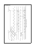
Physical Dimensions inches (millimeters) Cavity Dual-In-Line Package (J) Order Number TP3064J or TP3067J NS Package Number J20A Molded Small Outline Package (WM) Order Number TP3064WM or TP3067WM NS Package Number M20B 16
Physical Dimensions inches (millimeters) (Continued) Molded Dual-In-Line Package (N) Order Number TP3064N or TP3067N NS Package Number N20A 17
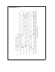
TP3064, TP3067 ‘‘Enhanced’’ Serial Interface CMOS CODEC/Filter COMBO Physical Dimensions inches (millimeters) (Continued) Lit. Ý 113975 Plastic Chip Carrier (V) Order Number TP3064V or TP3067V NS Package Number V20A LIFE SUPPORT POLICY NATIONAL’S PRODUCTS ARE NOT AUTHORIZED FOR USE AS CRITICAL COMPONENTS IN LIFE SUPPORT DEVICES OR SYSTEMS WITHOUT THE EXPRESS WRITTEN APPROVAL OF THE PRESIDENT OF NATIONAL SEMICONDUCTOR CORPORATION. As used herein: 1.
IMPORTANT NOTICE Texas Instruments Incorporated and its subsidiaries (TI) reserve the right to make corrections, modifications, enhancements, improvements, and other changes to its products and services at any time and to discontinue any product or service without notice. Customers should obtain the latest relevant information before placing orders and should verify that such information is current and complete.