TP3070,TP3070-X,TP3071 TP3070, TP3071, TP3070-X COMBO II Programmable PCM CODEC/Filter Literature Number: SNOSBX9
TP3070, TP3071, TP3070-X COMBO ® II Programmable PCM CODEC/Filter General Description Features The TP3070 and TP3071 are second-generation combined PCM CODEC and Filter devices optimized for digital switching applications on subscriber line and trunk cards. Using advanced switched capacitor techniques, COMBO II combines transmit bandpass and receive lowpass channel filters with a companding PCM encoder and decoder.
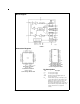
Block Diagram DS008635-1 FIGURE 1. Connection Diagrams DS008635-2 Order Number TP3071J See NS Package Number J20A Order Number TP3071N See NS Package Number N20A DS008635-4 Order Number TP3070V (0˚C to +70˚C) Order Number TP3070V-X (−40˚C to +85˚C) See NS Package Number V28A Pin Descriptions Pin VCC www.national.com 2 Description +5V ± 5% power supply. VBB −5V ± 5% power supply. GND Ground. All analog and digital signals are referenced to this pin. FSX Transmit Frame Sync input.
Pin Descriptions Pin FSR BCLK (Continued) Description Receive Frame Sync input. Normally a pulse or squarewave with an 8 kHz repetition rate is applied to this input to define the start of the receive time slot assigned to this device (non-delayed data timing mode), or the start of the receive frame (delayed data timing mode using the internal time-slot assignment counter). Bit clock input used to shift PCM data into and out of the DR and DX pins. BCLK may vary from 64 kHz to 4.
Functional Description A decode cycle begins immediately after the assigned receive time-slot, and 10 µs later the Decoder DAC output is updated. The total signal delay is 10 µs plus 120 µs (filter delay) plus 62.5 µs (1⁄2 frame) which gives approximately 190 µs.
Functional Description (Continued) TABLE 1.
Programmable Functions gains remain unchanged, thus care must be taken to ensure that overload levels are not exceeded anywhere in the loop. Hybrid balance must be disabled for meaningful analog loopback function. (Continued) vice is powered-up or down by setting the “P” bit as indicated. When the power-up or down control is entered as a single byte instruction, bit one (1) must be reset to a 0.
Programmable Functions (Continued) TABLE 5. Coding Law Conventions µ255 law MSB VIN = +Full Scale VIN = 0V VIN = −Full Scale True A-law with A-law without even bit inversion even bit inversion LSB MSB LSB MSB LSB 10000000 10101010 11111111 11111111 11010101 10000000 01111111 01010101 00000000 00000000 00101010 01111111 Note 5: The MSB is always the first PCM bit shifted in or out of COMBO II. TABLE 6.
Programmable Functions ator. Either of the filter sections can be bypassed if only one is required to achieve good cancellation. A selectable 180 degree inverting stage is included to compensate for interface circuits which also invert the transmit input relative to the receive output signal. The 2nd order section is intended mainly to balance low frequency signals across a transformer SLIC, and the first order section to balance midrange to higher audio frequency signals.
Programmable Functions (Continued) DS008635-5 FIGURE 2. Simplified Diagram of Hybrid Balance Circuit POWER SUPPLIES While the pins of the TP3070 COMBO II devices are well protected against electrical misuse, it is recommended that the standard CMOS practice of applying GND to the device before any other connections are made should always be followed.
Applications Information (Continued) DS008635-7 FIGURE 3. Typical Application with Monolithic SLIC www.national.
Absolute Maximum Ratings (Note 9) Storage Temperature Range VBB to GND Current at VFR0 Current at any Digital Output Lead Temperature (Soldering, 10 sec.) If Military/Aerospace specified devices are required, please contact the National Semiconductor Sales Office/ Distributors for availability and specifications. VCC to GND Voltage at VFXI Voltage at any Digital Input 7V VCC + 0.5V to VBB − 0.5V VCC + 0.5V to GND − 0.
Electrical Characteristics (Continued) Unless otherwise noted, limits printed in BOLD characters are guaranteed for VCC = +5V ± 5%, VBB = −5V ± 5%; TA = 0˚C to +70˚C (−40˚C to +85˚C for TP3070-X) by correlation with 100% electrical testing at TA = 25˚C. All other limits are assured by correlation with other production tests and/or product design and characterization. All signals referenced to GND. Typicals specified at VCC = +5V, VBB = −5V, TA = 25˚C.
Timing Specifications (Continued) Unless otherwise noted, limits printed in BOLD characters are guaranteed for VCC = +5V ± 5%; VBB = −5V ± 5%; TA = 0˚C to +70˚C (−40˚C to +85˚C for TP3070-X) by correlation with 100% electrical testing at TA = 25˚C. All other limits are assured by correlation with other production tests and/or product design and characterization. All signals referenced to GND. Typicals specified at VCC = +5V, VBB = −5V, TA = 25˚C. All timing parameters are measured at VOH = 2.
Timing Specifications (Continued) Unless otherwise noted, limits printed in BOLD characters are guaranteed for VCC = +5V ± 5%; VBB = −5V ± 5%; TA = 0˚C to +70˚C (−40˚C to +85˚C for TP3070-X) by correlation with 100% electrical testing at TA = 25˚C. All other limits are assured by correlation with other production tests and/or product design and characterization. All signals referenced to GND. Typicals specified at VCC = +5V, VBB = −5V, TA = 25˚C. All timing parameters are measured at VOH = 2.
Timing Diagrams (Continued) DS008635-9 FIGURE 5. Delayed Data Timing Mode (Time Slot Zero Only) 15 www.national.
(Continued) FIGURE 6. Control Port Timing DS008635-10 Timing Diagrams www.national.
Transmission Characteristics Unless otherwise noted, limits printed in BOLD characters are guaranteed for VCC = +5V ± 5%, VBB = −5V ± 5%; TA = 0˚C to +70˚C (−40˚C to +85˚C for TP3070-X) by correlation with 100% electrical testing at TA = 25˚C. f = 1015.625 Hz, VFXI = 0 dBm0, DR0 or DR1 = 0 dBm0 PCM code. Transmit and receive gains programmed for maximum 0 dBm0 test levels (0 dB gain), hybrid balance filter disabled.
Transmission Characteristics (Continued) Unless otherwise noted, limits printed in BOLD characters are guaranteed for VCC = +5V ± 5%, VBB = −5V ± 5%; TA = 0˚C to +70˚C (−40˚C to +85˚C for TP3070-X) by correlation with 100% electrical testing at TA = 25˚C. f = 1015.625 Hz, VFXI = 0 dBm0, DR0 or DR1 = 0 dBm0 PCM code. Transmit and receive gains programmed for maximum 0 dBm0 test levels (0 dB gain), hybrid balance filter disabled.
Transmission Characteristics (Continued) Unless otherwise noted, limits printed in BOLD characters are guaranteed for VCC = +5V ± 5%, VBB = −5V ± 5%; TA = 0˚C to +70˚C (−40˚C to +85˚C for TP3070-X) by correlation with 100% electrical testing at TA = 25˚C. f = 1015.625 Hz, VFXI = 0 dBm0, DR0 or DR1 = 0 dBm0 PCM code. Transmit and receive gains programmed for maximum 0 dBm0 test levels (0 dB gain), hybrid balance filter disabled.
Transmission Characteristics (Continued) Unless otherwise noted, limits printed in BOLD characters are guaranteed for VCC = +5V ± 5%, VBB = −5V ± 5%; TA = 0˚C to +70˚C (−40˚C to +85˚C for TP3070-X) by correlation with 100% electrical testing at TA = 25˚C. f = 1015.625 Hz, VFXI = 0 dBm0, DR0 or DR1 = 0 dBm0 PCM code. Transmit and receive gains programmed for maximum 0 dBm0 test levels (0 dB gain), hybrid balance filter disabled.
Transmission Characteristics (Continued) Unless otherwise noted, limits printed in BOLD characters are guaranteed for VCC = +5V ± 5%, VBB = −5V ± 5%; TA = 0˚C to +70˚C (−40˚C to +85˚C for TP3070-X) by correlation with 100% electrical testing at TA = 25˚C. f = 1015.625 Hz, VFXI = 0 dBm0, DR0 or DR1 = 0 dBm0 PCM code. Transmit and receive gains programmed for maximum 0 dBm0 test levels (0 dB gain), hybrid balance filter disabled.
Definitions and Timing Conventions DEFINITIONS VIH VIL VOH VIH is the D.C. input level above which an input level is guaranteed to appear as a logical one. This parameter is to be measured by performing a functional test at reduced clock speeds and nominal timing, (i.e., not minimum setup and hold times or output strobes), with the high level of all driving signals set to VIH and maximum supply voltages applied to the device. Pulse Width Low Setup Time VIL is the D.C.
23
Physical Dimensions inches (millimeters) unless otherwise noted Ceramic Dual-In-Line Package (J) Order Number TP3071J NS Package Number J20A Ceramic Dual-In-Line Package (J) Order Number TP3070J NS Package Number J28A www.national.
Physical Dimensions inches (millimeters) unless otherwise noted (Continued) Molded Dual-In-Line Package (N) Order Number TP3071N NS Package Number N20A 25 www.national.
TP3070, TP3071, TP3070-X COMBO II Programmable PCM CODEC/Filter Physical Dimensions inches (millimeters) unless otherwise noted (Continued) Plastic Leaded Chip Carrier (V) Order Number TP3070V or TP3070V-X NS Package Number V28A LIFE SUPPORT POLICY NATIONAL’S PRODUCTS ARE NOT AUTHORIZED FOR USE AS CRITICAL COMPONENTS IN LIFE SUPPORT DEVICES OR SYSTEMS WITHOUT THE EXPRESS WRITTEN APPROVAL OF THE PRESIDENT OF NATIONAL SEMICONDUCTOR CORPORATION. As used herein: 2.
IMPORTANT NOTICE Texas Instruments Incorporated and its subsidiaries (TI) reserve the right to make corrections, modifications, enhancements, improvements, and other changes to its products and services at any time and to discontinue any product or service without notice. Customers should obtain the latest relevant information before placing orders and should verify that such information is current and complete.