
User Manual


TPA005D02 Class D EVM PCB Layers
3-33
Details
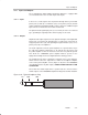
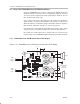
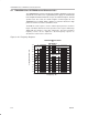
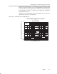
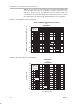
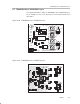
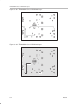
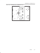
3.7 TPA005D02 Class D EVM PCB Layers
The following illustrations depict the TPA005D02 class D EVM PCB layers.
These drawings are not to scale. Gerber plots can be obtained from any TI
Sales Office.
Figure 3–26. TPA005D02 Class D EVM Silkscreen
Texas Instruments
1998
R6 R7
VDD
GND
L1
L2
L3
L4
U1
C21
C19
C15
+
TPA005D02 EVM Board Rev. A
VDD
GND
C25
Lout+
Lout–
Mute
Rout–
Rout+
C24
D2
D3
C4
C2
C3
C5
GND
RIN+
RIN–
C1
R2
R1
Q1
LIN–
LIN+
GND
Mute
S1
D1
C9
SLOP223
C7
C6
1
R3
+
C22
C23
C12
C10
C14
C13
C17
S2
C20
R4
R5
C8
C11
C27
C26
C16
C18
Shutdown
Figure 3–27. TPA005D02 Class D EVM Top Layer