
Datasheet

The TPA0212 Audio Power Amplifier Evaluation Module
3-4
Details
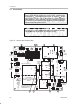
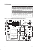
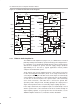
Figure 3–3. TPA0212 EVM Schematic Diagram
R4
100 kΩ
C12
10 µF
GNDGND
RLINEINGAIN0
SHUTDOWNGAIN1
ROUT+LOUT+
ROUT–LOUT–
SE/BTLLIN
PC–BEEPBYPASS
GNDGND
RHPINLLINEIN
V
DD
LHPIN
PV
DD
PV
DD
HP/LINERIN
10
9
12
11
6
5
8
7
2
1
4
3
23
22
21
20
19
18
17
16
15
14
13
24
S1
L OUT –
L OUT +
L HP
V
DD
C4
0.1 µF
R4
0 Ω
R LINE –
R OUT +
R HP
V
DD
ROUT–
SE/BTL
TPA0212
C11
0.47 µF
C8
0.47 µF
L IN +
C2
0.47 µF
R IN +
GND
C7
0.47 µF
C6
0.47 µF
L LINE –
S2
V
DD
S3
R3
100 kΩ
R2
100 kΩ
V
DD
R1
100 kΩ
C1
0.47 µF
SHUTDOWN
SHUTDOWN
C3
0.47 µF
C9
10 µF
GND
C5
0.1 µF
C10
0.47 µF
PCBEEP
V
DD
S4
R5
100 kΩ
S6
V
DD
S5
HP/LINE
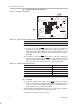
3.2.1 TPA0212 Audio Amplifier IC
The TPA0212 audio amplifier IC (Figure 3–4) is a CMOS device intended
primarily for bridge-tied load (BTL) operation in battery-powered applications.
It is supplied in a very small 24-pin TSSOP thermal surface-mount package
and has been designed to operate from low supply voltages (between
approximately 4.5 V and 5.5 V). Typical applications include portable
computers and multimedia systems.
The IC includes two separate amplifier channels, each of which can operate
in either the bridged-tied load (BTL) mode or the single-ended mode as
selected by the SE/BTL
pin. In the BTL mode, the line inputs are automatically
selected and the two output lines of each channel operate as mirror images
of each other for increased power. The speaker load is connected directly
across OUT+ and OUT–, and neither line is connected to ground. BTL
operation provides many benefits, including quadruple the output power of
single-ended operation and no need for bulky output coupling capacitors.
In the single-ended mode, the headphone inputs are automatically selected
and the speaker load is connected between the OUT+ terminal, through an
output coupling capacitor, to system ground. For more information, see the
TPA0212 amplifier IC data sheet, TI iiterature number SLOS284.