
Datasheet
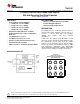
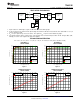


Input
Buffer
SC
300KΩ
EN
TPA2011D1
SLOS626A –DECEMBER 2009–REVISED MAY 2010
www.ti.com
OPERATING CHARACTERISTICS (continued)
V
DD
= 3.6 V, T
A
= 25°C, A
V
= 2 V/V, R
L
= 8 Ω (unless otherwise noted)
PARAMETER TEST CONDITIONS MIN TYP MAX UNIT
Time for which output is
disabled after a short-circuit
T
SD
event, after which V
DD
= 2.5 V to 5.5 V 100 ms
auto-recovery trials are
continuously made
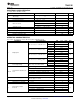
Terminal Functions
TERMINAL
I/O DESCRIPTION
NAME WCSP BALL
IN– C1 I Negative differential audio input
IN+ A1 I Positive differential audio input
V
O-
A3 O Negative BTL audio output
V
O+
C3 O Positive BTL audio output
Analog ground terminal. Must be connected to same potential as PGND using a direct connection
GND A2 I
to a single point ground.
High-current Analog ground terminal. Must be connected to same potential as GND using a direct
PGND B3 I
connection to a single point ground.
Power supply terminal. Must be connected to same power supply as PV
DD
using a direct
V
DD
B1 I
connection. Voltage must be within values listed in Recommended Operating Conditions table.
High-current Power supply terminal. Must be connected to same power supply as V
DD
using a
PV
DD
B2 I direct connection. Voltage must be within values listed in Recommended Operating Conditions
table.
EN C2 I Shutdown terminal. When terminal is low the device is put into Shutdown mode.
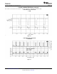
FUNCTIONAL BLOCK DIAGRAM
4 Submit Documentation Feedback Copyright © 2009–2010, Texas Instruments Incorporated
Product Folder Link(s) :TPA2011D1