
Datasheet
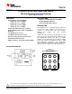
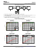


Measurement
Output
+
-
C
I
TPA2011D1
IN+
IN-
30 kHz
LowPass
Filter
Load
Measurement
Input
+
-
OUT+
OUT-
V
DD
GND
V
DD
C
S1
C
S2
C
I
+
-
R
I
R
I
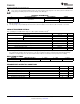
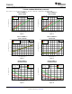
P
O
− Output Power − W
η − Efficiency − %
0.0 0.2 0.4 0.6 0.8 1.0 1.2 1.4 1.6 1.8 2.0
0
10
20
30
40
50
60
70
80
90
100
V
DD
= 2.5 V
V
DD
= 3.6 V
V
DD
= 5.0 V
R
L
= 8 Ω + 33 µH
Gain = 6 dB
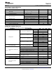
P
O
− Output Power − W
η − Efficiency − %
0.0 0.4 0.8 1.2 1.6 2.0 2.4 2.8 3.2 3.6
0
10
20
30
40
50
60
70
80
90
100
V
DD
= 2.5 V
V
DD
= 3.6 V
V
DD
= 5.0 V
R
L
= 4 Ω + 33 µH
Gain = 6 dB
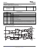
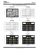
P
O
− Output Power − W
P
D
− Power Dissipation − W
0.0 0.2 0.4 0.6 0.8 1.0 1.2 1.4 1.6 1.8 2.0
0.0
0.1
0.2
0.3
0.4
R
L
= 8 Ω + 33 µH
R
L
= 4 Ω + 33 µH
V
DD
= 3.6 V
Gain = 6 dB
P
O
− Output Power − W
P
D
− Power Dissipation − W
0.0 0.4 0.8 1.2 1.6 2.0 2.4 2.8 3.2 3.6 4.0
0.0
0.1
0.2
0.3
0.4
0.5
0.6
R
L
= 8 Ω + 33 µH
R
L
= 4 Ω + 33 µH
V
DD
= 5.0 V
Gain = 6 dB
TPA2011D1
www.ti.com
SLOS626A –DECEMBER 2009–REVISED MAY 2010
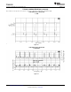
TEST SETUP FOR GRAPHS
1. Input resistor R
I
= 150kΩ gives a gain of 6 dB which is used for all the graphs
2. C
I
was shorted for any common-mode input voltage measurement. All other measurements were taken with C
I
= 0.1-mF
(unless otherwise noted).
3. C
S1
= 0.1mF is placed very close to the device. The optional C
S2
= 10mF is used for datasheet graphs.
4. The 30-kHz low-pass filter is required even if the analyzer has an internal low-pass filter. An RC low-pass filter (1kΩ,
4700pF) is used on each output for the data sheet graphs.
TYPICAL CHARACTERISTICS
V
DD
= 3.6 V, C
I
= 0.1 mF, C
S1
= 0.1 mF, C
S2
= 10 mF, T
A
= 25°C, R
L
= 8 Ω (unless otherwise noted)
EFFICIENCY vs EFFICIENCY vs
OUTPUT POWER OUTPUT POWER
Figure 1. Figure 2.
POWER DISSIPATION vs POWER DISSIPATION vs
OUTPUT POWER OUTPUT POWER
Figure 3. Figure 4.
Copyright © 2009–2010, Texas Instruments Incorporated Submit Documentation Feedback 5
Product Folder Link(s) :TPA2011D1