
Datasheet


TLV2731, TLV2731Y
Advanced LinCMOS RAIL-TO-RAIL
LOW-POWER SINGLE OPERATIONAL AMPLIFIERS
SLOS198A – AUGUST 1997 – REVISED MARCH 2001
1
POST OFFICE BOX 655303 • DALLAS, TEXAS 75265
Output Swing Includes Both Supply Rails
Low Noise . . . 15 nV/√Hz Typ at f = 1 kHz
Low Input Bias Current ...1 pA Typ
Fully Specified for Single-Supply 3-V and
5-V Operation
Common-Mode Input Voltage Range
Includes Negative Rail
High Gain Bandwidth ...2 MHz at
V
DD
= 5 V with 600 Ω Load
High Slew Rate . . . 1.6 V/µs at V
DD
= 5 V
Wide Supply Voltage Range
2.7 V to 10 V
Macromodel Included
description
The TLV2731 is a single low-voltage operational amplifier available in the SOT-23 package. It offers 2 MHz of
bandwidth and 1.6 V/µs of slew rate for applications requiring good ac performance. The device exhibits
rail-to-rail output performance for increased dynamic range in single or split supply applications. The TLV2731
is fully characterized at 3 V and 5 V and is optimized for low-voltage applications.
The TLV2731, exhibiting high input impedance and low noise, is excellent for small-signal conditioning of
high-impedance sources, such as piezoelectric transducers. Because of the micropower dissipation levels
combined with 3-V operation, these devices work well in hand-held monitoring and remote-sensing
applications. In addition, the rail-to-rail output feature with single- or split-supplies makes this family a great
choice when interfacing with analog-to-digital converters (ADCs). The device can also drive 600-Ω loads for
telecom applications.
With a total area of 5.6mm
2
, the SOT-23 package only requires one-third the board space of the standard 8-pin
SOIC package. This ultra-small package allows designers to place single amplifiers very close to the signal
source, minimizing noise pick-up from long PCB traces.
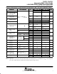
AVAILABLE OPTIONS
T
A
V
IO
max AT 25
°
C
PACKAGED DEVICES
SYMBOL
CHIP
FORM
‡
T
A
V
IO
max
AT
25°C
SOT-23 (DBV)
†
SYMBOL
FORM
‡
(Y)
0°C to 70°C 3 mV TLV2731CDBV VALC
TLV2731Y
–40°C to 85°C 3 mV TLV2731IDBV VALI
TLV2731Y
†
The DBV package available in tape and reel only.
‡
Chip forms are tested at T
A
= 25°C only.
Please be aware that an important notice concerning availability, standard warranty, and use in critical applications of
Texas Instruments semiconductor products and disclaimers thereto appears at the end of this data sheet.
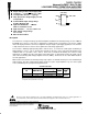
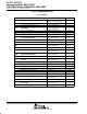
DBV PACKAGE
(TOP VIEW)
5
43
1
2
IN+
V
DD+
OUT V
DD–
/GND
IN–
PRODUCTION DATA information is current as of publication date.
Products conform to specifications per the terms of Texas Instruments
standard warranty. Production processing does not necessarily include
testing of all parameters.
Copyright 2001, Texas Instruments Incorporated
Advanced LinCMOS is a trademark of Texas Instruments.