SLOS386A − NOVEMBER 2001 − REVISED APRIL 2007 FEATURES D Internal Gain Control, Which Eliminates D D D D DESCRIPTION The TPA6017A2 is a stereo audio power amplifier in a 20-pin TSSOP thermally enhanced package capable of delivering 2 W of continuous RMS power per channel into 3-Ω loads. Internal gain control minimizes the number of external components needed, simplifying the design, and freeing up board space for other features.
SLOS386A − NOVEMBER 2001 − REVISED APRIL 2007 This integrated circuit can be damaged by ESD. Texas Instruments recommends that all integrated circuits be handled with appropriate precautions. Failure to observe proper handling and installation procedures can cause damage. AVAILABLE OPTIONS PACKAGED DEVICE† TA TSSOP (PWP) −40°C to 85°C TPA6017A2PWP † The PWP package is available taped and reeled. To order a taped and reeled part, add the suffix R to the part number (e.g., TPA6017A2PWPR).
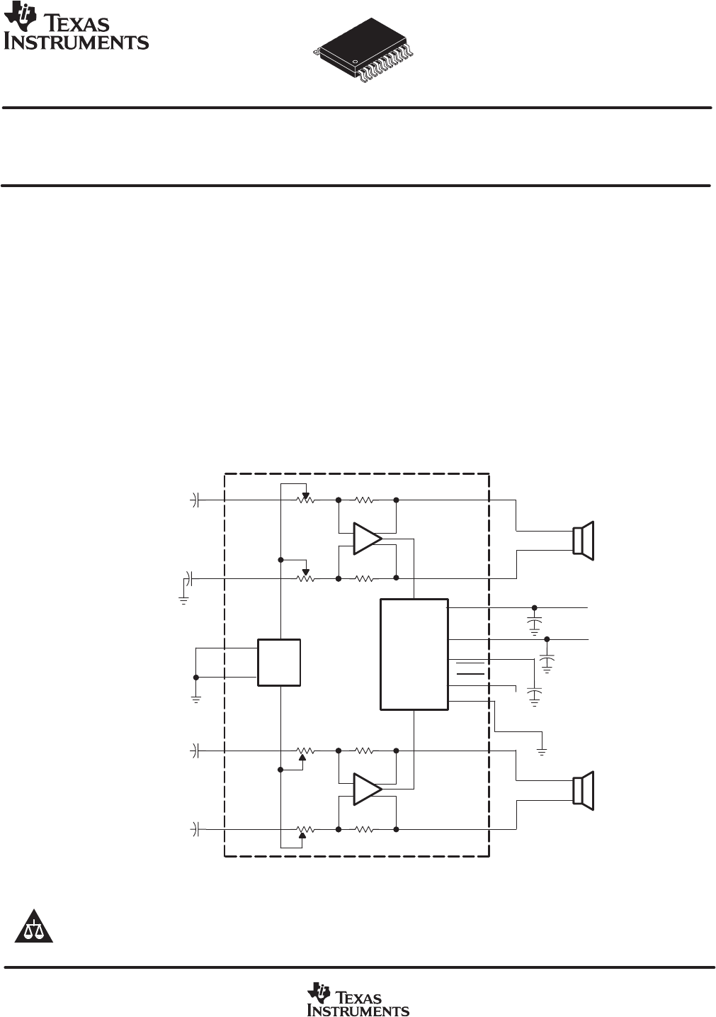
SLOS386A − NOVEMBER 2001 − REVISED APRIL 2007 functional block diagram RIN− − + ROUT+ − + ROUT− RIN+ Gain0 Gain1 Gain Control Depop Circuitry PVDD Power Management VDD BYPASS SHUTDOWN GND LIN− − + LOUT+ − + LOUT− LIN+ www.ti.
SLOS386A − NOVEMBER 2001 − REVISED APRIL 2007 absolute maximum ratings over operating free-air temperature range (unless otherwise noted)† Supply voltage, VDD . . . . . . . . . . . . . . . . . . . . . . . . . . . . . . . . . . . . . . . . . . . . . . . . . . . . . . . . . . . . . . . . . . . . . . . . . . . . . . 6 V Input voltage, VI . . . . . . . . . . . . . . . . . . . . . . . . . . . . . . . . . . . . . . . . . . . . . . . . . . . . . . . . . . . . . . . . . . −0.3 V to VDD +0.
SLOS386A − NOVEMBER 2001 − REVISED APRIL 2007 operating characteristics, VDD = 5 V, TA = 25°C, RL = 8 Ω, Gain = −2 V/V (unless otherwise noted) ÁÁÁÁÁÁÁÁÁÁÁÁÁÁÁÁÁÁÁÁÁÁÁÁÁÁÁÁÁÁÁÁÁÁÁÁÁÁÁÁ ÁÁÁÁÁÁÁÁÁÁÁÁÁÁÁÁÁÁÁÁÁÁÁÁÁÁÁÁÁÁÁÁÁÁÁÁÁÁÁÁ ÁÁÁÁÁÁÁÁÁÁÁÁÁÁÁÁÁÁÁÁÁÁÁÁÁÁÁÁÁÁÁÁÁÁÁÁÁÁÁÁ ÁÁÁÁÁÁÁÁÁÁÁÁÁÁÁÁÁÁÁÁÁÁÁÁÁÁÁÁÁÁÁÁÁÁÁÁÁÁÁÁ ÁÁÁÁÁÁÁÁÁÁÁÁÁÁÁÁÁÁÁÁÁÁÁÁÁÁÁÁÁÁÁÁÁÁÁÁÁÁÁÁ ÁÁÁÁÁÁÁÁÁÁÁÁÁÁÁÁÁÁÁÁÁÁÁÁÁÁÁÁÁÁÁÁÁÁÁÁÁÁÁ ÁÁÁÁÁÁÁÁÁÁÁÁÁÁÁÁÁÁÁÁÁÁÁÁÁÁÁÁÁÁÁÁÁÁÁÁÁÁÁ ÁÁÁÁÁÁÁÁÁÁÁÁÁÁÁÁÁÁÁÁÁÁÁÁÁÁÁÁÁÁÁÁÁÁÁÁÁÁÁ PARAMETER TEST CONDITIONS MIN
SLOS386A − NOVEMBER 2001 − REVISED APRIL 2007 TYPICAL CHARACTERISTICS TOTAL HARMONIC DISTORTION PLUS NOISE vs OUTPUT POWER TOTAL HARMONIC DISTORTION PLUS NOISE vs FREQUENCY 10% AV = 6 dB f = 1 kHz RL = 4 Ω 1% RL = 8 Ω RL = 3 Ω 0.1% 0.01% 0.5 0.75 1 1.25 1.5 1.75 2 PO = 1.75 W RL = 3 Ω THD+N −Total Harmonic Distortion + Noise THD+N −Total Harmonic Distortion + Noise 10% 2.25 2.5 2.75 1% 0.1% AV = 15.6 dB 0.
SLOS386A − NOVEMBER 2001 − REVISED APRIL 2007 TYPICAL CHARACTERISTICS TOTAL HARMONIC DISTORTION PLUS NOISE vs OUTPUT POWER TOTAL HARMONIC DISTORTION PLUS NOISE vs OUTPUT POWER 10% THD+N −Total Harmonic Distortion + Noise THD+N −Total Harmonic Distortion + Noise 10% f = 15 kHz 1% f = 1 kHz f = 20 Hz 0.1% RL = 3 Ω AV = 15.6 dB 0.01% 0.01 0.1 1 PO − Output Power − W f = 15 kHz 1% f = 1 kHz f = 20 Hz 0.1% RL = 3 Ω AV = 21.6 dB 0.01% 0.01 10 0.
SLOS386A − NOVEMBER 2001 − REVISED APRIL 2007 TYPICAL CHARACTERISTICS TOTAL HARMONIC DISTORTION PLUS NOISE vs OUTPUT POWER TOTAL HARMONIC DISTORTION PLUS NOISE vs OUTPUT POWER 10% RL = 4 Ω AV = 6 dB THD+N −Total Harmonic Distortion + Noise THD+N −Total Harmonic Distortion + Noise 10% f = 15 kHz 1% f = 1 kHz 0.1% f = 20 Hz 0.01% 0.01 0.1 1 PO − Output Power − W f = 15 kHz 1% f = 1 kHz 0.1% f = 20 Hz RL = 4 Ω AV = 15.6 dB 0.01% 0.01 10 0.
SLOS386A − NOVEMBER 2001 − REVISED APRIL 2007 TYPICAL CHARACTERISTICS TOTAL HARMONIC DISTORTION PLUS NOISE vs OUTPUT POWER TOTAL HARMONIC DISTORTION PLUS NOISE vs FREQUENCY 10% PO = 1 W RL = 8 Ω 1% AV = 21.6 dB AV = 6 dB 0.1% AV = 15.6 dB 0.01% 20 100 1k RL = 8 Ω AV = 6 dB THD+N −Total Harmonic Distortion + Noise THD+N −Total Harmonic Distortion + Noise 10% f = 1 kHz 0.1% f = 20 Hz 0.01% 0.01 10k 20k f − Frequency − Hz Figure 13 10% RL = 8 Ω AV = 15.
SLOS386A − NOVEMBER 2001 − REVISED APRIL 2007 TYPICAL CHARACTERISTICS OUTPUT NOISE VOLTAGE vs BANDWIDTH SUPPLY RIPPLE REJECTION RATIO vs FREQUENCY 100 Supply Ripple Rejection Ratio − dB 90 V n − Output Noise Voltage − µ V 0 VDD = 5 V RL = 4Ω 80 70 60 50 40 AV = 21.6 dB 30 AV = 15.6 dB 20 −20 RL = 8 Ω CB = 0.
SLOS386A − NOVEMBER 2001 − REVISED APRIL 2007 TYPICAL CHARACTERISTICS SIGNAL-TO-NOISE RATIO vs FREQUENCY 140 SNR − Signal-To-Noise Ratio − dB 130 PO = 1 W RL = 8 Ω 120 AV = 15.6 dB AV = 6 dB 110 100 90 AV = 21.6 dB 80 70 60 20 100 1k 10k 20k f − Frequency − Hz Figure 21 CLOSED LOOP RESPONSE 180° 10 7.5 Gain 90° 2.5 Phase 0 0° Phase Gain − dB 5 −2.5 −5 RL = 8 Ω AV = 6 dB −90° −7.5 −10 10 −180° 100 1k 10k 100k 1M f − Frequency − Hz Figure 22 www.ti.
SLOS386A − NOVEMBER 2001 − REVISED APRIL 2007 TYPICAL CHARACTERISTICS CLOSED LOOP RESPONSE 180° 30 25 90° 20 Phase 10 0° Phase Gain − dB Gain 15 5 0 RL = 8 Ω AV = 15.6 dB −90° −5 −10 10 −180° 100 1k 10k 100k 1M f − Frequency − Hz Figure 23 CLOSED LOOP RESPONSE 180° 30 25 Gain 90° 15 Phase 10 0° 5 0 RL = 8 Ω AV = 21.6 dB −90° −5 −10 10 −180° 100 1k 10k f − Frequency − Hz Figure 24 12 www.ti.
SLOS386A − NOVEMBER 2001 − REVISED APRIL 2007 TYPICAL CHARACTERISTICS POWER DISSIPATION vs OUTPUT POWER OUTPUT POWER vs LOAD RESISTANCE 1.8 3.5 AV = 6 dB 3Ω 1.6 PD − Power Dissipation − W 2.5 2 10% THD+N 1.5 1 1.4 1.2 4Ω 1 0.8 0.6 8Ω 0.4 f = 1 kHz Each Channel 1% THD+N 0.5 0.2 0 0 0 0 8 48 16 24 32 40 RL − Load Resistance − Ω 56 64 0.5 1 1.5 PO − Output Power − W Figure 25 2 2.
SLOS386A − NOVEMBER 2001 − REVISED APRIL 2007 THERMAL INFORMATION The thermally enhanced PWP package is based on the 20-pin TSSOP, but includes a thermal pad (see Figure 28) to provide an effective thermal contact between the IC and the PWB. Traditionally, surface-mount and power have been mutually exclusive terms. A variety of scaled-down TO-220-type packages have leads formed as gull wings to make them applicable for surface-mount applications.
SLOS386A − NOVEMBER 2001 − REVISED APRIL 2007 APPLICATION INFORMATION CRIN− Right 0.47 µF Line 17 Input Signal RIN− − + ROUT+ 18 − + ROUT− 14 CRIN+ 0.47 µF 7 2 3 RIN+ PVDD GAIN0 GAIN1 Gain Control Depop Circuitry Power Management Left Line Input Signal CLIN− 0.47 µF VDD 16 BYPASS SHUT− DOWN 10 GND 5 6,15 LIN− See Note A 19 To System Control − + LOUT+ 4 − + LOUT− 8 CSR 0.1 µF VDD VDD CSR 0.1 µF CBYP 0.47 µF 1,11, 13,20 CLIN+ 0.47 µF 9 NOTE A: LIN+ A 0.
SLOS386A − NOVEMBER 2001 − REVISED APRIL 2007 APPLICATION INFORMATION CRIN− Right 0.47 µF Negative 17 Differential Input Signal CRIN+ Right 0.47 µF Positive 7 Differential Input Signal 2 3 RIN− − + ROUT+ 18 − + ROUT− 14 RIN+ PVDD GAIN0 GAIN1 Gain Control Depop Circuitry Power Management CLIN− 0.47 µF Left Negative Differential Input Signal CLIN+ Left 0.
SLOS386A − NOVEMBER 2001 − REVISED APRIL 2007 APPLICATION INFORMATION shutdown modes The TPA6017A2 employs a shutdown mode of operation designed to reduce supply current, IDD, to the absolute minimum level during periods of nonuse for battery-power conservation. The SHUTDOWN input terminal should be held high during normal operation when the amplifier is in use. Pulling SHUTDOWN low causes the outputs to mute and the amplifier to enter a low-current state, IDD = 150 µA.
SLOS386A − NOVEMBER 2001 − REVISED APRIL 2007 APPLICATION INFORMATION input capacitor, CI (continued) The value of CI is important to consider as it directly affects the bass (low frequency) performance of the circuit. Consider the example where ZI is 10 kΩ, which is the absolute minimum input impedance of the TPA6017A2, and the specification calls for a flat bass response down to 40 Hz. Equation 2 is reconfigured as equation 2. 1 C + I 2p Z f c I (2) In this example, CI is 0.
SLOS386A − NOVEMBER 2001 − REVISED APRIL 2007 APPLICATION INFORMATION bridged-tied load versus single-ended mode Figure 31 shows a Class-AB audio power amplifier (APA) in a BTL configuration. The TPA6017A2 BTL amplifier consists of two Class-AB amplifiers driving both ends of the load. There are several potential benefits to this differential drive configuration, but initially consider power to the load.
SLOS386A − NOVEMBER 2001 − REVISED APRIL 2007 APPLICATION INFORMATION bridged-tied load versus single-ended mode (continued) For example, a 68-µF capacitor with an 8-Ω speaker would attenuate low frequencies below 293 Hz. The BTL configuration cancels the dc offsets, which eliminates the need for the blocking capacitors. Low-frequency performance is then limited only by the input network and speaker response. Cost and PCB space are also minimized by eliminating the bulky coupling capacitor.
SLOS386A − NOVEMBER 2001 − REVISED APRIL 2007 APPLICATION INFORMATION BTL amplifier efficiency (continued) Although the voltages and currents for SE and BTL are sinusoidal in the load, currents from the supply are very different between SE and BTL configurations. In an SE application, the current waveform is a half-wave rectified shape, whereas in BTL it is a full-wave rectified waveform. This means RMS conversion factors are different.
SLOS386A − NOVEMBER 2001 − REVISED APRIL 2007 APPLICATION INFORMATION BTL amplifier efficiency (continued) Table 2. Efficiency vs Output Power in 5-V 8-Ω BTL Systems Output Power (W) Efficiency (%) Peak Voltage (V) Internal Dissipation (W) 0.25 31.4 2.00 0.55 0.50 44.4 2.83 0.62 1.00 62.8 0.59 1.25 70.2 4.00 4.47† 0.53 † High peak voltages cause the THD to increase.
SLOS386A − NOVEMBER 2001 − REVISED APRIL 2007 APPLICATION INFORMATION crest factor and thermal considerations (continued) This is valuable information to consider when attempting to estimate the heat dissipation requirements for the amplifier system. Comparing the absolute worst case, which is 2 W of continuous power output with a 3 dB crest factor, against 12 dB and 15 dB applications drastically affects maximum ambient temperature ratings for the system.
SLOS386A − NOVEMBER 2001 − REVISED APRIL 2007 APPLICATION INFORMATION crest factor and thermal considerations (continued) T A Max + T J Max * Θ JA P D + 150 * 45 (0.6 2) + 96°C (18 dB crest factor) (11) NOTE: Internal dissipation of 0.6 W is estimated for a 2-W system with 18 dB crest factor per channel. Tables 3 and 4 show that for some applications no airflow is required to keep junction temperatures in the specified range.
PACKAGE OPTION ADDENDUM www.ti.
PACKAGE MATERIALS INFORMATION www.ti.com 14-Jul-2012 TAPE AND REEL INFORMATION *All dimensions are nominal Device TPA6017A2PWPR Package Package Pins Type Drawing SPQ HTSSOP 2000 PWP 20 Reel Reel A0 Diameter Width (mm) (mm) W1 (mm) 330.0 16.4 Pack Materials-Page 1 6.95 B0 (mm) K0 (mm) P1 (mm) 7.1 1.6 8.0 W Pin1 (mm) Quadrant 16.
PACKAGE MATERIALS INFORMATION www.ti.com 14-Jul-2012 *All dimensions are nominal Device Package Type Package Drawing Pins SPQ Length (mm) Width (mm) Height (mm) TPA6017A2PWPR HTSSOP PWP 20 2000 367.0 367.0 38.
IMPORTANT NOTICE Texas Instruments Incorporated and its subsidiaries (TI) reserve the right to make corrections, enhancements, improvements and other changes to its semiconductor products and services per JESD46C and to discontinue any product or service per JESD48B. Buyers should obtain the latest relevant information before placing orders and should verify that such information is current and complete.