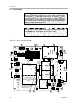
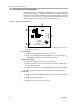
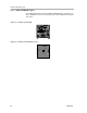
TPA751 EVM PCB Layers
2-8
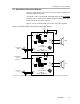
Operation
2.5.3 TPA751 EVM PCB Layers
The following illustrations depict the TPA751 EVM PCB layers and silkscreen.
These drawings are not to scale. Gerber plots can be obtained from any TI
sales office.
Figure 2–5. TPA751 EVM PCB
Figure 2–6. TPA751 EVM Bottom Layer