
Datasheet
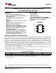


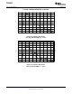
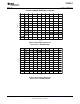


Table Of Contents
Ch2_Out
V
CC
(optional)
Ch1_Out
GND
Ch1_In
Ch2_In
ABSOLUTE MAXIMUM RATINGS
(1)
ESD RATINGS
TPD2S017
SLLS949 – SEPTEMBER 2009 ..........................................................................................................................................................................................
www.ti.com
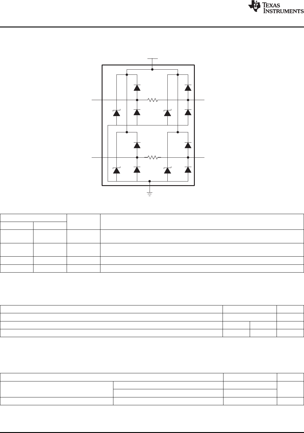
CIRCUIT DIAGRAM
TERMINAL FUNCTIONS
TERMINAL
I/O DESCRIPTION
NAME NO.
Ch1_In 3
I High-speed ESD clamp input
Ch2_In 4
Ch1_Out 1
O High-speed ESD clamp output
Ch2_Out 6
GND 2 – Ground
V
CC
5 – Optional power
over operating free-air temperature range (unless otherwise noted)
MIN MAX UNIT
V
IO
IO voltage range 0 5 V
T
stg
Storage temperature range – 85 125 ° C
TA Operating temperature – 40 85 ° C
(1) Stresses beyond those listed under " absolute maximum ratings " may cause permanent damage to the device. These are stress ratings
only, and functional operation of the device at these or any other conditions beyond those indicated under " recommended operating
conditions " is not implied. Exposure to absolute-maximum-rated conditions for extended periods may affect device reliability.
PARAMETER MIN MAX UNIT
Out pin ± 11
IEC 61000-4-2 Contact Discharge kV
In pin ± 11
Human Body Model In and out pins ± 15 kV
2 Submit Documentation Feedback Copyright © 2009, Texas Instruments Incorporated
Product Folder Link(s): TPD2S017