
Datasheet


TPD4E001
SLLS682K –JULY 2006–REVISED JANUARY 2015
www.ti.com
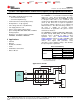
3. Ensure that there is enough metallization for the V
CC
and GND loop. During normal operation, the TPD4E001
consumes nA leakage current. But during the ESD event, V
CC
and GND may see 15 A to
30 A of current, depending on the ESD level. Sufficient current path enables safe discharge of all the energy
associated with the ESD strike.
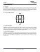
4. Leave the unused IO pins floating. In this example of protecting two USB ports, none of the IO pins will be
left unused.
5. The V
CC
pin can be connected in two different ways:
(a) If the V
CC
pin is connected to the system power supply, the TPD4E001 works as a transient suppressor
for any signal swing above V
CC
+ V
F
. A 0.1-μF capacitor on the device V
CC
pin is recommended for ESD
bypass.
(b) If the V
CC
pin is not connected to the system power supply, the TPD4E001 can tolerate higher signal
swing in the range up to 10 V. Please note that a 0.1-μF capacitor is still recommended at the V
CC
pin for
ESD bypass.
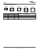
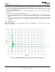
8.2.3 Application Curve
Figure 5 is a capture of the voltage clamping waveform of TPD4E001DRL on IO3 during a +8kV Contact
IEC61000-4-2 ESD strike.
Figure 5. TPD4E001DRL IEC61000-4-2 Voltage Clamp Waveform +8kV Contact
10 Submit Documentation Feedback Copyright © 2006–2015, Texas Instruments Incorporated
Product Folder Links: TPD4E001