
Datasheet


TPD4E001
SLLS682K –JULY 2006–REVISED JANUARY 2015
www.ti.com
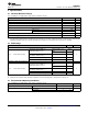
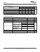
6.4 Thermal Information
TPD4E001
THERMAL METRIC
(1)
DRL DBV DCK DPK DRS UNIT
6 PINS
R
θJA
Junction-to-ambient thermal resistance 226.4 259.7 251.1 247.6 91.9
R
θJC(top)
Junction-to-case (top) thermal resistance 90.3 186.5 88.1 124.8 106.9
R
θJB
Junction-to-board thermal resistance 61.2 107.6 54.8 204.2 64.8
°C/W
ψ
JT
Junction-to-top characterization parameter 6.7 71.4 1.7 19.2 10.2
ψ
JB
Junction-to-board characterization parameter 61.0 107.1 54.1 209.3 64.9
R
θJC(bot)
Junction-to-case (bottom) thermal resistance N/A N/A N/A N/A 29.9
(1) For more information about traditional and new thermal metrics, see the IC Package Thermal Metrics application report, SPRA953.
6.5 Electrical Characteristics
over operating free-air temperature range (unless otherwise noted), V
CC
= 5 V ±10%
PARAMETER TEST CONDITIONS MIN TYP
(1)
MAX UNIT
V
CC
Supply voltage 0.9 5.5 V
I
CC
Supply current 1 100 nA
V
F
Diode forward voltage I
F
= 10 mA 0.65 0.95 V
V
BR
Breakdown Voltage I
BR
= 10 mA 11 V
Positive transients V
CC
+ 25
T
A
= 25°C, ±15-kV HBM,
I
F
= 10 A
Negative transients –25
T
A
= 25°C, Positive transients V
CC
+ 60
±8-kV Contact Discharge
Negative transients –60
(IEC 61000-4-2), I
F
= 24 A
V
C
Channel clamp voltage V
T
A
= 25°C, Positive transients V
CC
+ 100
±15-kV Air-Gap Discharge
Negative transients –100
(IEC 61000-4-2), I
F
= 45 A
Surge strike on IO pin,
GND pin grounded, Positive transients 17
I
PP
= 5A, 8/20 µs
(2)
V
RWM
Reverse stand-off voltage IO pin to GND pin 5.5 V
I
i/o
Channel leakage current V
i/o
= GND to V
CC
±1 nA
C
i/o
Channel input capacitance V
CC
= 5 V, Bias of V
CC
/2 1.5 pF
(1) Typical values are at V
CC
= 5 V and T
A
= 25°C.
(2) Non-repetitive current pulse 8/20 µs exponentially decaying waveform according to ICE61000-4-5.
6 Submit Documentation Feedback Copyright © 2006–2015, Texas Instruments Incorporated
Product Folder Links: TPD4E001