
Datasheet


SLIS095A − MARCH 2000 − REVISED MAY 2005
1
POST OFFICE BOX 655303 • DALLAS, TEXAS 75265
D Low r
DS(on)
...5 Ω
D Avalanche Energy . . . 30 mJ
D Eight Power DMOS-Transistor Outputs of
150-mA Continuous Current
D 500-mA Typical Current-Limiting Capability
D Output Clamp Voltage ...50 V
D Enhanced Cascading for Multiple Stages
D All Registers Cleared With Single Input
D Low Power Consumption
description
The TPIC6B596 is a monolithic, high-voltage,
medium-current power 8-bit shift register
designed for use in systems that require relatively
high load power. The device contains a built-in
voltage clamp on the outputs for inductive
transient protection. Power driver applications
include relays, solenoids, and other medium-
current or high-voltage loads.
This device contains an 8-bit serial-in, parallel-out
shift register that feeds an 8-bit D-type storage
register. Data transfers through both the shift and
storage registers on the rising edge of the
shift-register clock (SRCK) and the register clock
(RCK), respectively. The storage register
transfers data to the output buffer when shift-
register clear (SRCLR
) is high. When SRCLR is
low, all registers in the device are cleared. When
output enable (G
) is held high, all data in the
output buffers is held low and all drain outputs are
off. When G
is held low, data from the storage
register is transparent to the output buffers. When
data in the output buffers is low, the DMOS-
transistor outputs are off. When data is high, the
DMOS-transistor outputs have sink-current capability. The serial output (SER OUT) is clocked out of the device
on the falling edge of SRCK to provide additional hold time for cascaded applications. This will provide improved
performance for applications where clock signals may be skewed, devices are not located near one another,
or the system must tolerate electromagnetic interference.
Outputs are low-side, open-drain DMOS transistors with output ratings of 50 V and 150-mA continuous sink-
current capability. Each output provides a 500-mA typical current limit at T
C
= 25°C. The current limit decreases
as the junction temperature increases for additional device protection.
The TPIC6B596 is characterized for operation over the operating case temperature range of −40°C to 125°C.
Copyright 2000 − 2005, Texas Instruments Incorporated
! "#$ ! %#&'" ($)
(#"! " !%$""! %$ *$ $! $+! !#$!
!(( ,-) (#" %"$!!. ($! $"$!!'- "'#($
$!. '' %$$!)
Please be aware that an important notice concerning availability, standard warranty, and use in critical applications of
Texas Instruments semiconductor products and disclaimers thereto appears at the end of this data sheet.
1
2
3
4
5
6
7
8
9
10
20
19
18
17
16
15
14
13
12
11
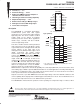
NC
V
CC
SER IN
DRAIN0
DRAIN1
DRAIN2
DRAIN3
SRCLR
G
GND
NC
GND
SER OUT
DRAIN7
DRAIN6
DRAIN5
DRAIN4
SRCK
RCK
GND
DW OR N PACKAGE
(TOP VIEW)
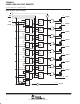
logic symbol
†
2
SRG8
†
This symbol is in accordance with ANSI/IEEE Std 91-1984
and IEC Publication 617-12.
9
12
8
13
3
EN3
C2
R
C1
1D
G
RCK
SRCLR
SRCK
SER IN
4
6
5
14
7
16
15
18
17
DRAIN0
DRAIN1
DRAIN2
DRAIN3
DRAIN4
DRAIN5
DRAIN6
DRAIN7
SER OUT
2
NC − No internal connection