
Datasheet

TPS2010, TPS2011, TPS2012, TPS2013
POWER-DISTRIBUTION
SLVS097A – DECEMBER 1994 – REVISED AUGUST 1995
1
POST OFFICE BOX 655303 • DALLAS, TEXAS 75265
95-mΩ Max (5.5-V Input) High-Side MOSFET
Switch With Logic Compatible Enable Input
Short-Circuit and Thermal Protection
Typical Short-Circuit Current Limits:
0.4 A, TPS2010; 1.2 A, TPS2011;
2 A, TPS2012; 2.6 A, TPS2013
Electrostatic-Discharge Protection, 12-kV
Output, 6-kV All Other Terminals
Controlled Rise and Fall Times to Limit
Current Surges and Minimize EMI
SOIC-8 Package Pin Compatible With the
Popular Littlefoot Series When GND Is
Connected
2.7-V to 5.5-V Operating Range
10-µA Maximum Standby Current
Surface-Mount SOIC-8 and TSSOP-14
Packages
–40°C to 125°C Operating Junction
Temperature Range
description
The TPS201x family of power-distribution switches is intended for applications where heavy capacitive loads
and short circuits are likely to be encountered. The high-side switch is a 95-mΩ N-channel MOSFET. Gate drive
is provided by an internal driver and charge pump designed to control the power switch rise times and fall times
to minimize current surges during switching. The charge pump operates at 100 kHz, requires no external
components, and allows operation from supplies as low as 2.7 V. When the output load exceeds the current-limit
threshold or a short circuit is present, the TPS201x limits the output current to a safe level by switching into a
constant-current mode. Continuous heavy overloads and short circuits increase power dissipation in the switch
and cause the junction temperature to rise. If the junction temperature reaches approximately 180°C, a thermal
protection circuit shuts the switch off to prevent damage. Recovery from thermal shutdown is automatic once
the device has cooled sufficiently.
The members of the TPS201x family differ only in short-circuit current threshold. The TPS2010 is designed to
limit at 0.4-A load; the other members of the family limit at 1.2 A, 2 A, and 2.6 A (see the available options table).
The TPS201x family is available in 8-pin small-outline integrated circuit (SOIC) and 14-pin thin shink
small-outline (TSSOP) packages and operates over a junction temperature range of –40°C to 125°C. Versions
in the 8-pin SOIC package are drop-in replacements for Siliconix’s Littlefoot power PMOS switches, except
that GND must be connected.
Copyright 1995, Texas Instruments Incorporated
PRODUCTION DATA information is current as of publication date.
Products conform to specifications per the terms of Texas Instruments
standard warranty. Production processing does not necessarily include
testing of all parameters.
Please be aware that an important notice concerning availability, standard warranty, and use in critical applications of
Texas Instruments semiconductor products and disclaimers thereto appears at the end of this data sheet.
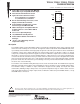
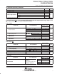
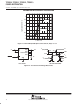
1
2
3
4
8
7
6
5
GND
IN
IN
EN
OUT
OUT
OUT
OUT
D PACKAGE
(TOP VIEW)
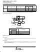
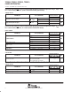
1
2
3
4
5
6
7
14
13
12
11
10
9
8
GND
IN
IN
IN
IN
IN
EN
OUT
OUT
OUT
OUT
OUT
OUT
OUT
PW PACKAGE
(TOP VIEW)