
Datasheet

TPS2042, TPS2052
DUAL POWER-DISTRIBUTION SWITCHES
SLVS173A – AUGUST 1998 – REVISED APRIL 1999
1
POST OFFICE BOX 655303 • DALLAS, TEXAS 75265
135-mΩ -Maximum (5-V Input) High-Side
MOSFET Switch
500 mA Continuous Current per Channel
Short-Circuit and Thermal Protection With
Overcurrent Logic Output
Operating Range . . . 2.7-V to 5.5-V
Logic-Level Enable Input
2.5-ms Typical Rise Time
Undervoltage Lockout
10 µA Maximum Standby Supply Current
Bidirectional Switch
Available in 8-pin SOIC and PDIP Packages
Ambient Temperature Range, –40°C to 85°C
2-kV Human-Body-Model, 200-V
Machine-Model ESD Protection
UL Listed – File No. E169910
description
The TPS2042 and TPS2052 dual power distribution switches are intended for applications where heavy
capacitive loads and short circuits are likely to be encountered. The TPS2042 and the TPS2052 incorporate
in single packages two 135-mΩ N-channel MOSFET high-side power switches for power distribution systems
that require multiple power switches. Each switch is controlled by a logic enable that is compatible with 5-V logic
and 3-V logic. Gate drive is provided by an internal charge pump designed to control the power-switch rise times
and fall times to minimize current surges during switching. The charge pump requires no external components
and allows operation from supplies as low as 2.7 V.
When the output load exceeds the current-limit threshold or a short is present, the TPS2042 and TPS2052 limit
the output current to a safe level by switching into a constant-current mode, pulling the overcurrent (OCx
) logic
output low. When continuous heavy overloads and short circuits increase the power dissipation in the switch
causing the junction temperature to rise, a thermal protection circuit shuts off the switch to prevent damage.
Recovery from a thermal shutdown is automatic once the device has cooled sufficiently. Internal circuitry
ensures the switch remains off until valid input voltage is present.
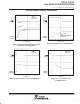
The TPS2042 and TPS2052 are designed to limit at 0.9-A load. These power distribution switches are available
in 8-pin small-outline integrated circuit (SOIC) and 8-pin plastic dual-in-line packages (PDIP) and operate over
an ambient temperature range of –40°C to 85°C.
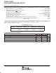
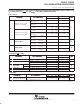
AVAILABLE OPTIONS
RECOMMENDED
MAXIMUM CONTINUOUS
TYPICAL
SHORT CIRCUIT CURRENT
PACKAGED DEVICES
T
A
ENABLE
MAXIMUM
CONTINUOUS
LOAD CURRENT
(A)
SHORT
-
CIRCUIT
CURRENT
LIMIT AT 25°C
(A)
SOIC
(D)
†
PDIP
(P)
–40°C to 85°C Active low 0.5 0.9 TPS2042D TPS2042P
–40°C to 85°C Active high 0.5 0.9 TPS2052D TPS2052P
†
The D package is available taped and reeled. Add an R suffix to device type (e.g., TPS2042DR)
Copyright 1999, Texas Instruments Incorporated
PRODUCTION DATA information is current as of publication date.
Products conform to specifications per the terms of Texas Instruments
standard warranty. Production processing does not necessarily include
testing of all parameters.
Please be aware that an important notice concerning availability, standard warranty, and use in critical applications of
Texas Instruments semiconductor products and disclaimers thereto appears at the end of this data sheet.
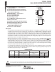
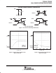
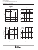
1
2
3
4
8
7
6
5
GND
IN
EN1
EN2
OC1
OUT1
OUT2
OC2
TPS2042
D OR P PACKAGE
(TOP VIEW)
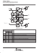
1
2
3
4
8
7
6
5
GND
IN
EN1
EN2
OC1
OUT1
OUT2
OC2
TPS2052
D OR P PACKAGE
(TOP VIEW)