
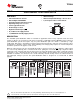
Datasheet
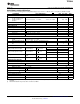

ABSOLUTE MAXIMUM RATINGS
DISSIPATING RATING TABLE
RECOMMENDED OPERATING CONDITIONS
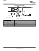
TPS2049
SLVS713A – OCTOBER 2006 – REVISED SEPTEMBER 2007 .........................................................................................................................................
www.ti.com
These devices have limited built-in ESD protection. The leads should be shorted together or the device placed in conductive foam
during storage or handling to prevent electrostatic damage to the MOS gates.
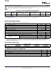
AVAILABLE OPTION AND ORDERING INFORMATION
(1)
RECOMMENDED MAXIMUM TYPICAL SHORT-CIRCUIT
NUMBER OF
T
A
ENABLE CONTINUOUS LOAD CURRENT CURRENT LIMIT AT 25 ° C SOIC (D)
SWITCHES
(mA) (mA)
– 40 ° C to 85 ° C Active low 100 150 Single TPS2049D
(2)
(1) For the most current package and ordering information, see the Package Option Addendum at the end of this document, or see the TI
website at www.ti.com .
(2) The package is available taped and reeled. Add an R suffix to device types (e.g., TPS2042BDR)
over operating free-air temperature range unless otherwise noted
(1)
VALUE UNIT
V
I(IN)
Input voltage range
(2)
– 0.3 to 6 V
V
O(OUT)
Output voltage range
(2)
-0.3 to 6 V
V
I( EN)
Input voltage range – 0.3 to 6 V
V
I( OC)
Voltage range – 0.3 to 6 V
I
O(OUT)
Continuous output current Internally limited
Continuous total power dissipation See Dissipation Rating Table
T
J
Operating virtual junction temperature range – 40 to 125 ° C
T
stg
Storage temperature range – 65 to 150 ° C
Lead temperature soldering 1,6 mm (1/16 inch) from case for 10 seconds 260 ° C
Human body model MIL-STD-883C 2 kV
Electrostatic discharge (ESD)
protection
Charge device model (CDM) 500 V
(1) Stresses beyond those listed under absolute maximum ratings may cause permanent damage to the device. These are stress ratings
only, and functional operation of the device at these or any other conditions beyond those indicated under recommended operating
conditions is not implied. Exposure to absolute-maximum-rated conditions for extended periods may affect device reliability.
(2) All voltages are with respect to GND.
T
A
≤ 25 ° C DERATING FACTOR T
A
= 70 ° C T
A
= 85 ° C
PACKAGE
POWER RATING ABOVE T
A
= 25 ° C POWER RATING POWER RATING
D-8 585.82 mW 5.8582 mW/C 322.20 mW 234.32 mW
MIN MAX UNIT
V
I(IN)
Input voltage 2.7 5.5 V
V
I( EN)
Input voltage 0 5.5 V
I
O(OUT)
Continuous output current 0 100 mA
T
J
Operating virtual junction temperature – 40 125 ° C
2 Submit Documentation Feedback Copyright © 2006 – 2007, Texas Instruments Incorporated
Product Folder Link(s): TPS2049