
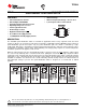
Datasheet
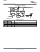

POWER DISSIPATION AND JUNCTION TEMPERATURE
THERMAL PROTECTION
UNDERVOLTAGE LOCKOUT (UVLO)
TPS2049
SLVS713A – OCTOBER 2006 – REVISED SEPTEMBER 2007 .........................................................................................................................................
www.ti.com
The low on-resistance on the n-channel MOSFET allows small surface-mount packages to pass large currents.
The thermal resistance of these packages are high compared to those of power packages; it is good design
practice to check power dissipation and junction temperature. Begin by determining the r
DS(on)
of the N-channel
MOSFET relative to the input voltage and operating temperature. As an initial estimate, use the highest operating
ambient temperature of interest. Using this value, the power dissipation per switch can be calculated by:
P
D
= r
DS(on)
× I
2
Finally, calculate the junction temperature:
T
J
= P
D
× R
Θ JA
+ T
A
Where:
T
A
= Ambient temperature ° C
R
Θ JA
= Thermal resistance
P
D
= Total power dissipation based on number of switches being used.
Compare the calculated junction temperature with the initial estimate. If they do not agree within a few degrees,
repeat the calculation, using the calculated value as the new estimate. Two or three iterations are generally
sufficient to get a reasonable answer.
Thermal protection prevents damage to the IC when heavy-overload or short-circuit faults are present for
extended periods of time. The TPS2049 implement a thermal sensing to monitor the operating junction
temperature of the power distribution switch. In an overcurrent or short-circuit condition the junction temperature
will rise due to excessive power dissipation. Once the die temperature rises to approximately 140 ° C due to
overcurrent conditions, the internal thermal sense circuitry turns the power switch off, thus preventing the power
switch from damage. Hysteresis is built into the thermal sense circuit, and after the device has cooled
approximately 10 ° C, the switch turns back on. The switch continues to cycle in this manner until the load fault or
input power is removed. The OC open-drain output is asserted (active low) when an overtemperature shutdown
or overcurrent occurs.
An undervoltage lockout ensures that the power switch is in the off state at power up. Whenever the input
voltage falls below approximately 2 V, the power switch will be quickly turned off. This facilitates the design of
hot-insertion systems where it is not possible to turn off the power switch before input power is removed. The
UVLO will also keep the switch from being turned on until the power supply has reached at least 2 V, even if the
switch is enabled. Upon reinsertion, the power switch will be turned on, with a controlled rise time to reduce EMI
and voltage overshoots.
8 Submit Documentation Feedback Copyright © 2006 – 2007, Texas Instruments Incorporated
Product Folder Link(s): TPS2049