
Datasheet
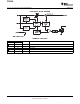
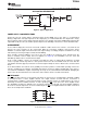
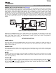

GENERIC HOT-PLUG APPLICATIONS (see Figure 8 )
DETAILED DESCRIPTION
POWER SWITCH
CHARGE PUMP
DRIVER
ENABLE ( EN)
TPS2049
www.ti.com
......................................................................................................................................... SLVS713A – OCTOBER 2006 – REVISED SEPTEMBER 2007
In many applications it may be necessary to remove modules or pc boards while the main unit is still operating.
These are considered hot-plug applications. Such implementations require the control of current surges seen by
the main power supply and the card being inserted. The most effective way to control these surges is to limit and
slowly ramp the current and voltage being applied to the card, similar to the way in which a power supply
normally turns on. Due to the controlled rise times and fall times of the TPS2049, these devices can be used to
provide a softer start-up to devices being hot-plugged into a powered system. The UVLO feature of the TPS2049
also ensures the switch will be off after the card has been removed, and the switch will be off during the next
insertion. The UVLO feature insures a soft start with a controlled rise time for every insertion of the card or
module.
Figure 8. Typical Hot-Plug Implementation
By placing the TPS2049 between the V
CC
input and the rest of the circuitry, the input power reaches these
devices first after insertion. The typical rise time of the switch is approximately 1 ms, providing a slow voltage
ramp at the output of the device. This implementation controls system surge currents and provides a
hot-plugging mechanism for any device.
The power switch is an N-channel MOSFET with a low on-state resistance. Configured as a high-side switch, the
power switch prevents current flow from OUT to IN and IN to OUT when disabled. The power switch supplies a
minimum current of 90 mA.
An internal charge pump supplies power to the driver circuit and provides the necessary voltage to pull the gate
of the MOSFET above the source. The charge pump operates from input voltages as low as 2.7 V and requires
little supply current.
The driver controls the gate voltage of the power switch. To limit large current surges and reduce the associated
electromagnetic interference (EMI) produced, the driver incorporates circuitry that controls the rise times and fall
times of the output voltage.
The logic enable pin disables the power switch and the bias for the charge pump, driver, and other circuitry to
reduce the supply current. The supply current is reduced to less than 1 µ A when a logic high is present on EN. A
logic zero input on EN restores bias to the drive and control circuits and turns the switch on. The enable input is
compatible with both TTL and CMOS logic levels.
Copyright © 2006 – 2007, Texas Instruments Incorporated Submit Documentation Feedback 9
Product Folder Link(s): TPS2049