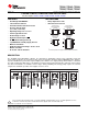
TPS2061, TPS2062, TPS2063 TPS2065, TPS2066, TPS2067 www.ti.com SLVS490I – DECEMBER 2003 – REVISED OCTOBER 2009 CURRENT-LIMITED, POWER-DISTRIBUTION SWITCHES Check for Samples: TPS2061 TPS2062 TPS2063 TPS2065 TPS2066 TPS2067 FEATURES APPLICATIONS • • • • • • 1 2 • • • • • • • • • • 70-mΩ High-Side MOSFET 1-A Continuous Current Thermal and Short-Circuit Protection Accurate Current Limit (1.1 A min, 1.9 A max) Operating Range: 2.7 V to 5.5 V 0.
TPS2061, TPS2062, TPS2063 TPS2065, TPS2066, TPS2067 SLVS490I – DECEMBER 2003 – REVISED OCTOBER 2009 www.ti.com This integrated circuit can be damaged by ESD. Texas Instruments recommends that all integrated circuits be handled with appropriate precautions. Failure to observe proper handling and installation procedures can cause damage. ESD damage can range from subtle performance degradation to complete device failure.
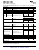
TPS2061, TPS2062, TPS2063 TPS2065, TPS2066, TPS2067 www.ti.com SLVS490I – DECEMBER 2003 – REVISED OCTOBER 2009 ABSOLUTE MAXIMUM RATINGS over operating free-air temperature range unless otherwise noted (1) UNIT Input voltage range, VI(IN) (2) Output voltage range, VO(OUT) -0.3 V to 6 V (2) -0.3 V to 6 V , VO(OUTx) Input voltage range, VI(EN), VI(EN), VI(ENx), VI(ENx) -0.3 V to 6 V Voltage range, VI(OC), VI(OCx) -0.
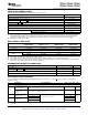
TPS2061, TPS2062, TPS2063 TPS2065, TPS2066, TPS2067 SLVS490I – DECEMBER 2003 – REVISED OCTOBER 2009 www.ti.com ELECTRICAL CHARACTERISTICS (continued) over recommended operating junction temperature range, VI(IN) = 5.5 V, IO = 1 A, VI(ENx) = 0 V, or VI(ENx) = 5.5 V (unless otherwise noted) PARAMETER TEST CONDITIONS (1) MIN TYP MAX UNIT ENABLE INPUT EN OR EN VIH High-level input voltage 2.7 V ≤ VI(IN) ≤ 5.5 V VIL Low-level input voltage 2.7 V ≤ VI(IN) ≤ 5.
TPS2061, TPS2062, TPS2063 TPS2065, TPS2066, TPS2067 www.ti.
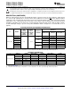
TPS2061, TPS2062, TPS2063 TPS2065, TPS2066, TPS2067 SLVS490I – DECEMBER 2003 – REVISED OCTOBER 2009 www.ti.com Pin Functions (TPS2062 and TPS2066) PINS NAME I/O NO.
TPS2061, TPS2062, TPS2063 TPS2065, TPS2066, TPS2067 www.ti.
TPS2061, TPS2062, TPS2063 TPS2065, TPS2066, TPS2067 SLVS490I – DECEMBER 2003 – REVISED OCTOBER 2009 www.ti.
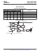
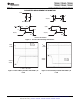
TPS2061, TPS2062, TPS2063 TPS2065, TPS2066, TPS2067 www.ti.com SLVS490I – DECEMBER 2003 – REVISED OCTOBER 2009 PARAMETER MEASUREMENT INFORMATION OUT RL tf tr CL VO(OUT) 90% 90% 10% 10% TEST CIRCUIT 50% VI(EN) 50% toff ton VO(OUT) 50% VI(EN) 90% 50% toff ton 90% VO(OUT) 10% 10% VOLTAGE WAVEFORMS Figure 1.
TPS2061, TPS2062, TPS2063 TPS2065, TPS2066, TPS2067 SLVS490I – DECEMBER 2003 – REVISED OCTOBER 2009 www.ti.com PARAMETER MEASUREMENT INFORMATION (continued) RL = 5 W, CL = 100 mF TA = 255C VI(EN) 5 V/div VI(EN) 5 V/div RL = 5 W, CL = 100 mF TA = 255C VO(OUT) 2 V/div VO(OUT) 2 V/div t − Time − 500 ms/div t − Time − 500 ms/div Figure 4. Turnon Delay and Rise Time With 100-μF Load VI(EN) 5 V/div Figure 5.
TPS2061, TPS2062, TPS2063 TPS2065, TPS2066, TPS2067 www.ti.com SLVS490I – DECEMBER 2003 – REVISED OCTOBER 2009 PARAMETER MEASUREMENT INFORMATION (continued) VO(OC) 2 V/div VO(OC) 2 V/div IO(OUT) 1 A/div IO(OUT) 1 A/div t − Time − 2 ms/div t − Time − 2 ms/div Figure 8. 2-Ω Load Connected to Enabled Device Figure 9. 1-Ω Load Connected to Enabled Device TYPICAL CHARACTERISTICS TURNON TIME vs INPUT VOLTAGE TURNOFF TIME vs INPUT VOLTAGE 1.0 2 CL = 100 mF, RL = 5 W, TA = 255C 0.9 0.
TPS2061, TPS2062, TPS2063 TPS2065, TPS2066, TPS2067 SLVS490I – DECEMBER 2003 – REVISED OCTOBER 2009 www.ti.com TYPICAL CHARACTERISTICS (continued) RISE TIME vs INPUT VOLTAGE FALL TIME vs INPUT VOLTAGE 0.25 0.6 0.5 0.2 0.4 Fall Time − ms Rise Time − ms CL = 1 mF, RL = 5 W, TA = 255C CL = 1 mF, RL = 5 W, TA = 255C 0.3 0.15 0.1 0.2 0.05 0.1 0 2 3 4 5 VI − Input Voltage − V 0 6 2 Figure 13.
TPS2061, TPS2062, TPS2063 TPS2065, TPS2066, TPS2067 www.ti.com SLVS490I – DECEMBER 2003 – REVISED OCTOBER 2009 TYPICAL CHARACTERISTICS (continued) TPS2063, TPS2067 SUPPLY CURRENT, OUTPUT ENABLED vs JUNCTION TEMPERATURE TPS2061, TPS2065 SUPPLY CURRENT, OUTPUT DISABLED vs JUNCTION TEMPERATURE 80 VI = 5.5 V 70 VI = 5 V 60 VI = 3.3 V 50 40 VI = 2.7 V 30 20 10 0 −50 I I (IN) − Supply Current, Output Disabled − µ A I I (IN) − Supply Current, Output Disabled − µ A 0.
TPS2061, TPS2062, TPS2063 TPS2065, TPS2066, TPS2067 SLVS490I – DECEMBER 2003 – REVISED OCTOBER 2009 www.ti.com TYPICAL CHARACTERISTICS (continued) STATIC DRAIN-SOURCE ON-STATE RESISTANCE vs JUNCTION TEMPERATURE SHORT-CIRCUIT OUTPUT CURRENT vs JUNCTION TEMPERATURE 1.56 120 IO = 0.5 A I OS − Short-Circuit Output Current − A On-State Resistance − mΩ 100 r DS(on) − Static Drain-Source VI = 2.7 V 1.54 Out1 = 5 V Out1 = 3.3 V 80 Out1 = 2.7 V 60 40 20 1.52 VI = 3.3 V 1.5 1.48 1.46 1.44 VI = 5 V 1.
TPS2061, TPS2062, TPS2063 TPS2065, TPS2066, TPS2067 www.ti.com SLVS490I – DECEMBER 2003 – REVISED OCTOBER 2009 TYPICAL CHARACTERISTICS (continued) CURRENT-LIMIT RESPONSE vs PEAK CURRENT 200 Current-Limit Response − µ s VI = 5 V, TA = 255C 150 100 50 0 0 Copyright © 2003–2009, Texas Instruments Incorporated 2.5 5 7.5 Peak Current − A Figure 24. 10 12.
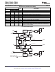
TPS2061, TPS2062, TPS2063 TPS2065, TPS2066, TPS2067 SLVS490I – DECEMBER 2003 – REVISED OCTOBER 2009 www.ti.com APPLICATION INFORMATION POWER-SUPPLY CONSIDERATIONS TPS2062 2 Power Supply 2.7 V to 5.5 V IN OUT1 0.1 µF 8 3 5 4 7 Load 0.1 µF 22 µF 0.1 µF 22 µF OC1 EN1 OUT2 6 OC2 Load EN2 GND 1 Figure 25. Typical Application A 0.01-μF to 0.1-μF ceramic bypass capacitor between IN and GND, close to the device, is recommended.
TPS2061, TPS2062, TPS2063 TPS2065, TPS2066, TPS2067 www.ti.com SLVS490I – DECEMBER 2003 – REVISED OCTOBER 2009 V+ TPS2062 GND Rpullup OC1 IN OUT1 EN1 OUT2 EN2 OC2 Figure 26. Typical Circuit for the OC Pin POWER DISSIPATION AND JUNCTION TEMPERATURE The low on-resistance on the N-channel MOSFET allows the small surface-mount packages to pass large currents.
TPS2061, TPS2062, TPS2063 TPS2065, TPS2066, TPS2067 SLVS490I – DECEMBER 2003 – REVISED OCTOBER 2009 www.ti.com UNDERVOLTAGE LOCKOUT (UVLO) An undervoltage lockout ensures that the power switch is in the off state at power up. Whenever the input voltage falls below approximately 2 V, the power switch is quickly turned off. This facilitates the design of hot-insertion systems where it is not possible to turn off the power switch before input power is removed.
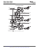
TPS2061, TPS2062, TPS2063 TPS2065, TPS2066, TPS2067 www.ti.com SLVS490I – DECEMBER 2003 – REVISED OCTOBER 2009 Downstream USB Ports D+ D− VBUS 0.1 µF 33 µF GND Power Supply 3.3 V 5V D+ TPS2062 2 IN OUT1 0.1 µF VBUS 0.1 µF 8 3 USB Controller D− 7 5 4 33 µF GND OC1 EN1 D+ OC2 EN2 OUT2 GND D− 6 VBUS 0.1 µF 33 µF GND 1 D+ D− VBUS 0.1 µF 33 µF GND Figure 27. Typical Four-Port USB Host / Self-Powered Hub BPHs obtain all power from upstream ports and often contain an embedded function.
TPS2061, TPS2062, TPS2063 TPS2065, TPS2066, TPS2067 SLVS490I – DECEMBER 2003 – REVISED OCTOBER 2009 Power Supply 3.3 V D+ D− VBUS www.ti.com TPS2062 2 10 µF 0.1 µF IN OUT1 GND 8 3 USB Control 5 4 7 0.1 µF 10 µF Internal Function 0.1 µF 10 µF Internal Function OC1 EN1 OC2 EN2 OUT2 GND 1 6 Figure 28.
TPS2061, TPS2062, TPS2063 TPS2065, TPS2066, TPS2067 www.ti.com SLVS490I – DECEMBER 2003 – REVISED OCTOBER 2009 TUSB2040 Hub Controller Upstream Port SN75240 BUSPWR A C B D GANGED D+ D− DP0 DP1 DM0 DM1 Tie to TPS2041 EN Input D+ 5V IN DM2 5-V Power Supply EN 33 µF† DM3 D+ A C B D 1 µF TPS76333 4.7 µF 5V DP3 OUT 0.1 µF D− SN75240 Ferrite Beads GND DP4 IN 3.3 V 4.
TPS2061, TPS2062, TPS2063 TPS2065, TPS2066, TPS2067 SLVS490I – DECEMBER 2003 – REVISED OCTOBER 2009 www.ti.com PC Board TPS2062 OC1 GND Power Supply 2.7 V to 5.5 V 1000 µF Optimum 0.1 µF IN EN1 EN2 Block of Circuitry OUT1 OUT2 OC2 Block of Circuitry Overcurrent Response Figure 30. Typical Hot-Plug Implementation By placing the TPS206x between the VCC input and the rest of the circuitry, the input power reaches these devices first after insertion.
TPS2061, TPS2062, TPS2063 TPS2065, TPS2066, TPS2067 www.ti.com SLVS490I – DECEMBER 2003 – REVISED OCTOBER 2009 Current Sense A sense FET monitors the current supplied to the load. The sense FET measures current more efficiently than conventional resistance methods. When an overload or short circuit is encountered, the current-sense circuitry sends a control signal to the driver.
TPS2061, TPS2062, TPS2063 TPS2065, TPS2066, TPS2067 SLVS490I – DECEMBER 2003 – REVISED OCTOBER 2009 www.ti.com Changes from Revision F (April 2008) to Revision G • Page Changed DBV-5 to Product Preview. ................................................................................................................................... 1 Changes from Revision G (July 2008) to Revision H Page • Deleted Product Preview from the DBV package .................................................................
PACKAGE OPTION ADDENDUM www.ti.
PACKAGE OPTION ADDENDUM www.ti.
PACKAGE OPTION ADDENDUM www.ti.
PACKAGE OPTION ADDENDUM www.ti.com 18-Oct-2013 (3) MSL, Peak Temp. - The Moisture Sensitivity Level rating according to the JEDEC industry standard classifications, and peak solder temperature. (4) There may be additional marking, which relates to the logo, the lot trace code information, or the environmental category on the device. (5) Multiple Device Markings will be inside parentheses. Only one Device Marking contained in parentheses and separated by a "~" will appear on a device.
PACKAGE MATERIALS INFORMATION www.ti.com 30-Dec-2013 TAPE AND REEL INFORMATION *All dimensions are nominal Device Package Package Pins Type Drawing SPQ TPS2061DBVR SOT-23 3000 179.0 DBV 5 Reel Reel A0 Diameter Width (mm) (mm) W1 (mm) B0 (mm) K0 (mm) P1 (mm) 8.4 3.2 3.2 1.4 4.0 W Pin1 (mm) Quadrant 8.0 Q3 TPS2061DBVT SOT-23 DBV 5 250 179.0 8.4 3.2 3.2 1.4 4.0 8.0 Q3 TPS2061DGNR MSOPPower PAD DGN 8 2500 330.0 12.4 5.3 3.4 1.4 8.0 12.
PACKAGE MATERIALS INFORMATION www.ti.com 30-Dec-2013 Device Package Package Pins Type Drawing SPQ Reel Reel A0 Diameter Width (mm) (mm) W1 (mm) B0 (mm) K0 (mm) P1 (mm) W Pin1 (mm) Quadrant PAD TPS2065DGNR MSOPPower PAD DGN 8 2500 330.0 12.4 5.3 3.3 1.3 8.0 12.0 Q1 TPS2065DR SOIC D 8 2500 330.0 12.4 6.4 5.2 2.1 8.0 12.0 Q1 TPS2066DGNR MSOPPower PAD DGN 8 2500 330.0 12.4 5.3 3.3 1.3 8.0 12.0 Q1 TPS2066DGNR MSOPPower PAD DGN 8 2500 330.0 12.4 5.3 3.4 1.
PACKAGE MATERIALS INFORMATION www.ti.com 30-Dec-2013 Device Package Type Package Drawing Pins SPQ Length (mm) Width (mm) Height (mm) TPS2062DR SOIC D 8 2500 340.5 338.1 20.6 TPS2063DR SOIC D 16 2500 367.0 367.0 38.0 TPS2065DBVR SOT-23 DBV 5 3000 180.0 180.0 18.0 TPS2065DBVR SOT-23 DBV 5 3000 203.0 203.0 35.0 TPS2065DBVT SOT-23 DBV 5 250 180.0 180.0 18.0 TPS2065DBVT SOT-23 DBV 5 250 203.0 203.0 35.0 TPS2065DGNR MSOP-PowerPAD DGN 8 2500 364.
IMPORTANT NOTICE Texas Instruments Incorporated and its subsidiaries (TI) reserve the right to make corrections, enhancements, improvements and other changes to its semiconductor products and services per JESD46, latest issue, and to discontinue any product or service per JESD48, latest issue. Buyers should obtain the latest relevant information before placing orders and should verify that such information is current and complete.