
Datasheet
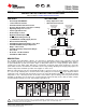
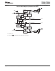
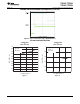

D−8 DRB−8DGN−8
TPS2060/TPS2064
DGNPACKAGE
(TOP VIEW)
GND
1
2
3
4
8
7
6
5
IN
EN1
EN2
OC1
OUT1
OUT2
OC2
TPS2068
DGNPACKAGE
(TOP VIEW)
GND
1
2
3
4
8
7
6
5
IN
IN
EN
OUT
OUT
OUT
OC
TPS2069
DGNPACKAGE
(TOP VIEW)
GND
1
2
3
4
8
7
6
5
IN
IN
EN
OUT
OUT
OUT
OC
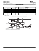
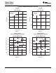
TPS2068
DPACKAGE
(TOP VIEW)
GND
IN
IN
EN
OUT
OUT
OUT
OC
1
2
3
4
8
7
6
5
GND
IN
EN1
†
EN2
OC1
OUT1
OUT2
OC2
TPS2060/TPS2064
DRBPACKAGES
(TOP VIEW)
† Allenableinputsareactivehighforthe TPS2064devices.
†
†
†
4
3
2
1
5
6
7
8
TPS2060, TPS2064
TPS2068, TPS2069
www.ti.com
SLVS553K – MARCH 2005– REVISED MAY 2011
CURRENT-LIMITED, POWER-DISTRIBUTION SWITCHES
Check for Samples: TPS2060, TPS2064, TPS2068, TPS2069
1
FEATURES
APPLICATIONS
2
• 70-mΩ High-Side MOSFET
• Heavy Capacitive Loads
• 1.5-A Continuous Current • Short-Circuit Protections
• Thermal and Short-Circuit Protection
• Accurate Current Limit (1.6 A min, 2.6 A max)
• Operating Range: 2.7 V to 5.5 V
• 0.6-ms Typical Rise Time
• Undervoltage Lockout
• Deglitched Fault Report (OC)
• No OC Glitch During Power Up
• 1-μA Maximum Standby Supply Current
• Reverse Current Blocking
• TPS2060/64 Temperature Range: 0°C to 70°C
• TPS2068/69 DGN Package Temperature
Range: –40°C to 85°C
• TPS2068 D Package Temperature Range:
0°C to 70°C
• UL Listed – File No. E169910
• TPS2068/69: CB Certified
DESCRIPTION
The TPS206x power-distribution switches are intended for applications where heavy capacitive loads and
short-circuits are likely to be encountered. This device incorporates 70-mΩ N-channel MOSFET power switches
for power-distribution systems that require single or dual power switches in a single package. Each switch is
controlled by a logic enable input. Gate drive is provided by an internal charge pump designed to control the
power-switch rise times and fall times to minimize current surges during switching. The charge pump requires no
external components and allows operation from supplies as low as 2.7 V.
When the output load exceeds the current-limit threshold or a short is present, the device limits the output current
to a safe level by switching into a constant-current mode, pulling the overcurrent (OCx) logic output low. When
continuous heavy overloads and short-circuits increase the power dissipation in the switch, causing the junction
temperature to rise, a thermal protection circuit shuts off the switch to prevent damage. Recovery from a thermal
shutdown is automatic once the device has cooled sufficiently. Internal circuitry ensures that the switch remains
off until valid input voltage is present. Current limit is typically 2.1 A.
1
Please be aware that an important notice concerning availability, standard warranty, and use in critical applications of Texas
Instruments semiconductor products and disclaimers thereto appears at the end of this data sheet.
2PowerPad is a trademark of Texas Instruments.
PRODUCTION DATA information is current as of publication date.
Copyright © 2005–2011, Texas Instruments Incorporated
Products conform to specifications per the terms of the Texas
Instruments standard warranty. Production processing does not
necessarily include testing of all parameters.