
Datasheet

SLVS333 − AUGUST 2001
1
www.ti.com
FEATURES
D
Two 340-mΩ (Typical) High-Side MOSFETs
D 200 mA Low-Dropout Voltage Regulator In
Fixed 3.3-V or Adjustable Versions
D Independent Thermal- and Short-Circuit
Protection for LDO and Each Switch
D Overcurrent Indicators With Transient Filter
D 2.9-V to 5.5-V Operating Range
D CMOS- and TTL-Compatible Enable Inputs
D 75-µA (Typical) Supply Current
D Available in 10-Pin MSOP or 14-Pin TSSOP
(PowerPAD)
D −40°C to 85°C Ambient Temperature Range
APPLICATIONS
D
USB Hubs and Peripherals
− Keyboards
− Zip Drives
− Speakers and Headsets
D PDAs and Portable Electronics
D DSP Power Sequencing
DESCRIPTION
Two power-distribution switches and an adjustable
(TPS2145) or fixed (TPS2147) LDO are incorporated in
one small package, providing a power management
solution that saves up to 60% in board space over
typical implementations.
Designed to meet USB 2.0 bus-powered hub
requirements, these devices also allow core and I/O
voltage sequencing in DSP applications, or power
segmentation in portable equipment. Each current-
limited switch is a 340-mΩ N-channel MOSFET capable
of supplying 200 mA of continuous current. A logic
enable compatible with 5-V logic and 3-V logic controls
each MOSFET as well as the LDO in the TPS2145. The
internal charge pump provides the gate drive controlling
the power-switch rise times and fall times, minimizing
current surges during switching. The charge pump
requires no external components.
The LDO has a drop-out voltage of only 0.35 V and with
the independent enable on the TPS2145 LDO, the LDO
can be used as an additional switch. The LDO output
range for the TPS2145 is 1 V to 3.3 V, while the
TPS2147 is fixed at 3.3 V.
The TPS2145 and TPS2147 have active-low switch
enables and the TPS2155 and TPS2157 have
active-high switch enables.
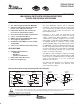
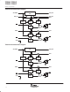
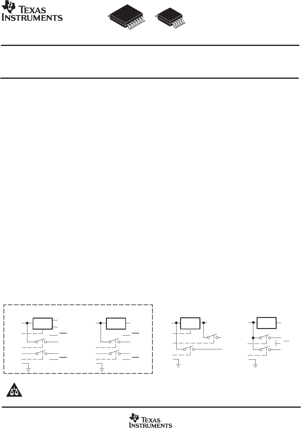
LDO and dual switch family selection guide and schematics
LDO
LDO_OUT
LDO_ADJ
OC1
OUT1
OUT2
OC2
VIN/SW1
LDO_EN
EN1
SW2
EN2
GND
TPS2145/55
TSSOP−14
LDO
OC1
OC2
EN1
SW2
EN2
GND
TPS2147/57
MSOP−10
LDO
EN2
EN1
GND
TPS2148/58
MSOP−8
LDO
OC
EN1
EN2
GND
TPS2149/59
MSOP−8
VIN/SW1
LDO_OUT
OUT1
OUT2
VIN/SW1
LDO_EN
LDO_OUT
OUT2
OUT1
VIN
LDO_OU
T
OUT1
OUT2
! " #$%! " &$'(#! )!%*
)$#!" # ! "&%##!" &% !+% !%" %," "!$%!"
"!)) -!.* )$#! &#%""/ )%" ! %#%""(. #($)%
!%"!/ (( &%!%"*
PowerPAD is a trademark of Texas Instruments.
Copyright 2001, Texas Instruments Incorporated
Please be aware that an important notice concerning availability, standard warranty, and use in critical applications of
Texas Instruments semiconductor products and disclaimers thereto appears at the end of this data sheet.