
Datasheet

SLVS399A − JANUARY 2002 − REVISED MAY 2006
1
www.ti.com
FEATURES
D
Complete Power Management Solution for
USB High-Power Peripherals
D 250 mA Low-Dropout Regulator (LDO) With
Enable and 325 mA (Typ) Current Limit
D LDO Supports 2.7 V to 5.5 V V
IN
and 0.9 V to
3.3 V Adjustable V
OUT
D 40 mΩ (Typ) High-Side MOSFET With Dual
Current Limit
D Undervoltage Lockout and Power Good for
LDO and Switch
D CMOS- and TTL-Compatible Enable Inputs
D 85 µA (Typ) Supply Current
D 5 µA (Typ) Standby Supply Current
D Available in 14-Pin HTSSOP (PowerPAD)
D −40°C to +85°C Ambient Temperature Range
D Alternative to TPS2148/58 3.3-V LDO With
3.3-V Switch and 5-V Switch
APPLICATIONS
D
High-Power USB Peripherals
− ADSL Modems
− Digital Still and PC Cameras
− Zip Drives
− Speakers
D DSP Sequencing
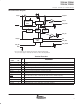
DESCRIPTION
The TPS2140/41/50/51 is a USB 1.0 and 2.0
Specification-compatible IC containing a dual-current-
limiting power switch and an adjustable low dropout
regulator (LDO). Both the switch and LDO limit inrush
current by controlling the turnon slew rate. The unique
dual-current-limiting feature of the switch allows USB
peripherals to utilize high-value capacitance at the
output of the switch, while keeping the inrush current
low. During turnon, the switch limits the current
delivered to the capacitive load to less than 100 mA.
When the output voltage from the switch reaches about
93% of the input voltage, the switch power good output
goes high, and the switch current limit increases to
800mA (minimum), at which point higher current loads
can be turned on. The higher current limit provides short
circuit protection while allowing the peripheral to draw
maximum current from the USB bus.
The switch and LDO function independently, providing
flexibility in DSP applications requiring separate core
and I/O voltages. For example, in a DSP application
operating from a 3.3-V rail, the LDO can supply the DSP
core voltage down to 0.9 V, while the switch powers the
3.3-V (typical) DSP I/O supply. If supply sequencing is
required, the LDO power good output can be used to
enable the switch.
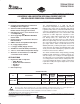
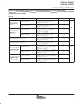
AVAILABLE OPTIONS
TARGET
PACKAGE
PACKAGED DEVICES
T
A
DESCRIPTION
TARGET
APPLICATION
PACKAGE
AND PIN
COUNT
ACTIVE LOW
(SWITCH)
ACTIVE HIGH
(SWITCH)
−40°C to 85°C
Adjustable LDO and 3.3 V switch with dual current
limit
DSP HTSSOP-14 TPS2140IPWP TPS2150IPWP
−40°C to 85°C
Adjustable LDO and 5 V switch with dual current
limit
USB HTSSOP-14 TPS2141IPWP TPS2151IPWP
NOTE: All options available taped and reeled. Add an R suffix (e.g., TPS2140IPWPR)
!"#$ % &'!!($ #% )'*+&#$ ,#$(-
!,'&$% &!" $ %)(&&#$% )(! $.( $(!"% (/#% %$!'"($%
%$#,#!, 0#!!#$1- !,'&$ )!&(%%2 ,(% $ (&(%%#!+1 &+',(
$(%$2 #++ )#!#"($(!%-
Copyright 2000−2006, Texas Instruments Incorporated
Please be aware that an important notice concerning availability, standard warranty, and use in critical applications of
Texas Instruments semiconductor products and disclaimers thereto appears at the end of this data sheet.
PowerPAD is a trademark of Texas Instruments. USB is a trademark of Universal Serial Bus Association.
All other trademarks are the property of their respective owners.