
Datasheet
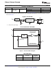
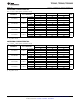
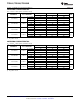


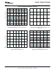
Table Of Contents
- FEATURES
- APPLICATIONS
- DESCRIPTION
- ABSOLUTE MAXIMUM RATINGS
- THERMAL IMPEDANCE RATINGS
- RECOMMENDED OPERATING CONDITIONS
- ELECTRICAL CHARACTERISTICS
- SWITCHING CHARACTERISTICS
- SWITCHING CHARACTERISTICS
- SWITCHING CHARACTERISTICS
- SWITCHING CHARACTERISTICS
- SWITCHING CHARACTERISTICS
- SWITCHING CHARACTERISTICS
- TYPICAL CHARACTERISTICS
- PARAMETER MEASUREMENT INFORMATION
- APPLICATION INFORMATION
- REVISION HISTORY
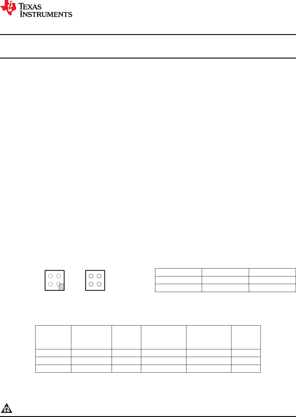
Laser Marking View
Bump View
B
2 1
A
B
1 2
A
TPS22901, TPS22902, TPS22902B
www.ti.com
SLVS803C –NOVEMBER 2008–REVISED DECEMBER 2012
ULTRA SMALL, LOW INPUT VOLTAGE, LOW r
ON
, LOAD SWITCHES
Check for Samples: TPS22901, TPS22902, TPS22902B
1
FEATURES
APPLICATIONS
• Low Input Voltage: 1.0 V to 3.6 V • Personal Digital Assistants (PDAs)
• Ultra-Low ON Resistance • Cellular Phones
– r
ON
= 78 mΩ at V
IN
= 3.6 V • GPS Devices
– r
ON
= 93 mΩ at V
IN
= 2.5 V • MP3 Players
– r
ON
= 109 mΩ at V
IN
= 1.8 V • Digital Cameras
– r
ON
= 146 mΩ at V
IN
= 1.2 V • Peripheral Ports
• 500-mA Maximum Continuous Switch Current • Portable Instrumentation
• Ultra Low Quiescent Current: 82 nA at 1.8 V • RF Modules
• Ultra Low Shutdown Current: 44 nA at 1.8 V
DESCRIPTION
• Low Control Input Thresholds Enable Use of
TPS22901, TPS22902, and TPS22902B are ultra-
1.2-V/1.8-V/2.5-V/3.3-V Logic
small, low ON resistance (r
ON
) load switches with
• Controlled Slew Rate to Avoid Inrush Currents
controlled turn on. The devices contain a P-channel
– TPS22901 and TPS22902: 40-μs t
r
MOSFET that operates over an input voltage range of
1.0 V to 3.6 V. The switch is controlled by an on/off
– TPS22902B: 220-μs t
r
input (ON), which is capable of interfacing directly
• ESD Performance Tested Per JESD 22
with low-voltage control signals. In TPS22902 and in
– 2000-V Human-Body Model
TPS22902B, a 120-Ω on-chip load resistor is added
(A114-B, Class II)
for output quick discharge when the switch is turned
off.
– 1000-V Charged-Device Model (C101)
TPS22901, TPS22902, and TPS22902B are available
• Four-Terminal Wafer-Chip-Scale Package
in a space-saving 4-terminal WCSP with 0.4-mm
(WCSP)
pitch (YFP). The devices are characterized for
– 0.8 mm × 0.8 mm, 0.4 mm Pitch,
operation over the free-air temperature range of
0.5 mm Height
–40°C to 85°C.
Table 1. TERMINAL ASSIGNMENTS
YFP PACKAGE
B ON GND
A V
IN
V
OUT
2 1
SLEW
r
ON
at 1.8 V RATE QUICK OUTPUT MAX OUTPUT
ENABLE
(TYP) (TYP at DISCHARGE
(1)
CURRENT
1.8 V)
TPS22901 109 mΩ 40 μs 500 mA Active high
TPS22902 109 mΩ 40 μs Yes 500 mA Active high
TPS22902B 109 mΩ 220 μs Yes 500 mA Active high
(1) This feature discharges the output of the switch to ground through a 120-Ω resistor, preventing the
output from floating.
1
Please be aware that an important notice concerning availability, standard warranty, and use in critical applications of
Texas Instruments semiconductor products and disclaimers thereto appears at the end of this data sheet.
PRODUCTION DATA information is current as of publication date.
Copyright © 2008–2012, Texas Instruments Incorporated
Products conform to specifications per the terms of the Texas
Instruments standard warranty. Production processing does not
necessarily include testing of all parameters.