
Datasheet
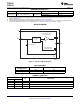
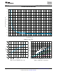

Bump View
1
2
B
A
Laser Marking View
2
1
B
A
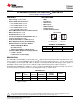
TPS22903
TPS22904
www.ti.com
SLVS827C –FEBRUARY 2009–REVISED APRIL 2010
ULTRA-SMALL LOW-INPUT-VOLTAGE LOW r
ON
LOAD SWITCH
Check for Samples: TPS22903, TPS22904
1
FEATURES
APPLICATIONS
• PDAs
• Input Voltage: 1.1 V to 3.6 V
• Cell Phones
• Ultra-Low ON-State Resistance
• GPS Devices
– r
ON
= 66 mΩ at V
IN
= 3.6 V
• MP3 Players
– r
ON
= 75 mΩ at V
IN
= 2.5 V
• Digital Cameras
– r
ON
= 90 mΩ at V
IN
= 1.8 V
• Peripheral Ports
– r
ON
= 135 mΩ at V
IN
= 1.2 V
• Portable Instrumentation
• 500-mA Maximum Continuous Switch Current
YFP PACKAGE
• Quiescent Current < 1 mA
• Shutdown Current < 1 mA
• Low Control Input Threshold Enables Use of
1.2-V/1.8-V/2.5-V/3.3-V Logic
• Controlled Slew Rate (5 ms Max at 3.6 V)
• Quick Output Discharge (TPS22904 Only)
• ESD Performance Tested Per JESD 22
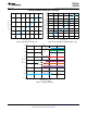
TERMINAL ASSIGNMENTS
– 2000-V Human-Body Model
B GND ON
(A114-B, Class II)
A V
OUT
V
IN
– 1000-V Charged-Device Model (C101)
2 1
• 4-Terminal Wafer Chip-Scale Package (WCSP)
– 0.8 mm × 0.8 mm,
0.4-mm Pitch, 0.5-mm Height
DESCRIPTION
The TPS22903 and TPS22904 are ultra-small, low r
ON
single channel load switches with controlled turn on. The
device contains a P-channel MOSFET that can operate over an input voltage range of 1.1 V to 3.6 V. The switch
is controlled by an on/off input (ON), which is capable of interfacing directly with low-voltage control signals. In
TPS22904, a 85-Ω on-chip load resistor is added for output quick discharge when switch is turned off.
TPS22903 and TPS22904 are available in a space-saving 4-terminal WCSP 0.4-mm pitch (YFP). The devices
are characterized for operation over the free-air temperature range of –40°C to 85°C.
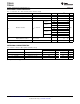
FEATURE LIST
MAXIMUM
r
ON
TYPICAL SLEW RATE QUICK OUTPUT
DEVICE OUTPUT ENABLE
AT 3.6 V AT 3.6 V DISCHARGE
(1)
CURRENT
TPS22903 66 mΩ 5 ms max No 500 mA Active high
TPS22904 66 mΩ 5 ms max Yes 500 mA Active high
(1) This feature discharges the output of the switch to ground through a 85-Ω resistor, preventing the
output from floating.
1
Please be aware that an important notice concerning availability, standard warranty, and use in critical applications of Texas
Instruments semiconductor products and disclaimers thereto appears at the end of this data sheet.
PRODUCTION DATA information is current as of publication date.
Copyright © 2009–2010, Texas Instruments Incorporated
Products conform to specifications per the terms of the Texas
Instruments standard warranty. Production processing does not
necessarily include testing of all parameters.