
Datasheet

www.ti.com
Operation
3 Operation
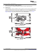
Connect the positive input of the power supply to the VIN J1 and the negative lead of the power supply to
GND J3. The input voltage range of the TPS2291xx is 1.4 V to 5.5 V.
Output load can be applied by connecting between J4 VOUT and J6 GND. The TPS2291xx is rated for a
maximum continuous current of 2A. Configure jumper JP3 as required. JP3 must be installed for proper
operation. When the ON pin is asserted, the TPS2291xx will control the slew rate of VOUT. The slew rate
of the device is internally controlled to avoid inrush current. When ON is deasserted, the TPS2291xx will
open the P-Channel MOSFET. Devices equipped with the Quick Output Discharge (QOD) option will
connect a 150Ω on-chip load resistor to the output for quick discharge. Devices equipped with the QOD
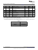
function are noted in Table 1.
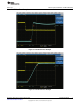
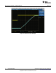
4 Test Results
See the Typical Characteristics section of the TPS2291xx data sheet.
3
SLVU501A–August 2011–Revised January 2012 TPS2291xxEVM-656
Submit Documentation Feedback
Copyright © 2011–2012, Texas Instruments Incorporated