
Datasheet

User's Guide
SLVU456B–May 2011–Revised May 2013
TPS22924EVM-532
This user's guide describes the characteristics, operation, and use of the TPS22924EVM-532 evaluation
module (EVM). This EVM demonstrates the Texas Instruments TPS22924 load switch with controlled turn
on. The input voltage range of the TPS22924 is 0.75 V to 3.6 V. An integrated charge pump biases the
NMOS switch to achieve a minimum switch ON resistance. The switch is controlled by an on/off input
(EN), which is capable of interfacing directly with low-voltage control signals. This user's guide includes
setup instructions, schematic diagram, bill of materials, and printed-circuit board layout drawings for the
EVM.
1 Introduction
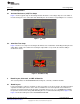
The TPS22924EVM-532 evaluation module (EVM) helps designers evaluate the operation and
performance of the TPS22924 load switch. The board features the small 6-pin CSP package for a small
solution size.
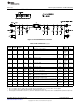
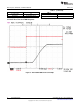
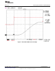
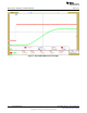
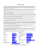
Table 1. TPS22924 VOUT Rise Time Options
EVM Device Rise Time VIN (V) Max. Enable (ON Quick
(µs) Typical Continuous Pin) Output
Current Discharge
HPA532-001 TPS22924B 100 3.6 2-A Active High Yes
HPA532-002 TPS22924C 840 3.6 2-A Active High Yes
HPA532-003 TPS22924D 6200 3.6 2-A Active High Yes
1.1 Related Documentation From Texas Instruments
TPS22924, ULTRA-SMALL, LOW-INPUT-VOLTAGE, LOW r
ON
LOAD SWITCH data sheets (SLVSA52,
SLVSAR3, SLVSBT4)
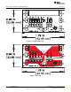
2 Setup
This section describes the jumpers and connectors on the EVM as well as how to properly connect, set
up, and use the TPS22924EVM-532.
2.1 J1/J3 – Input Connections
This is the connection for the leads from the input source. Connect the positive connection to the VIN J1
and the negative connection to the GND J3.
2.2 J4/J6 – Output Connections
This is the connection for the output of the TPS22924EVM. Connect the positive connection of the load to
the VOUT J4 and the negative connection to the GND J6.
1
SLVU456B–May 2011–Revised May 2013 TPS22924EVM-532
Submit Documentation Feedback
Copyright © 2011–2013, Texas Instruments Incorporated