
Datasheet


1
2
3
4
5
6
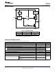
VIN
GND
VIN
VOUT
GND
ON
TPS22929
SLVSB39 –DECEMBER 2011
www.ti.com
These devices have limited built-in ESD protection. The leads should be shorted together or the device placed in conductive foam
during storage or handling to prevent electrostatic damage to the MOS gates.
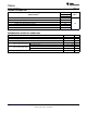
ORDERING INFORMATION
ORDERABLE PART
T
A
PACKAGE
(1)
TOP-SIDE MARKING
NUMBER
TPS22929ADBVT
TPS22929ADBVR
TPS22929BDBVT
Contact factory for Contact factory for
availability
(2)
availability
(2)
TPS22929BDBVR
–40°C to 85°C DBV
TPS22929CDBVT
TPS22929CDBVR
Tape of 3000 TPS22929DDBVT
_F4_
Reel of 250 TPS22929DDBVR
(1) Package drawings, standard packing quantities, thermal data, symbolization, and PCB design guidelines are available at
www.ti.com/sc/package.
(2) Contact factory for details and availability for PREVIEW devices, minimum order quantities may apply.
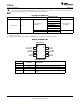
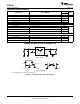
DEVICE INFORMATION
DBV PACKAGE
PIN FUNCTIONS
TPS22929
PIN NAME DESCRIPTION
DBV
2, 5 GND Ground
3 ON Switch control input, active high. Do not leave floating
1 VOUT Switch output
Switch input, bypass this input with a ceramic capacitor to
4, 6 VIN
ground
2 Submit Documentation Feedback Copyright © 2011, Texas Instruments Incorporated
Product Folder Link(s) :TPS22929