
Datasheet
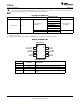
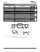

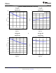

Control
Logic
ON
GND
UVLO
Reverse
Current
Protection
V
IN
V
OUT
TPS22929
www.ti.com
SLVSB39 –DECEMBER 2011
BLOCK DIAGRAM
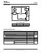
Table 2. FUNCTION TABLE
ON VIN to VOUT VOUT to GND
(1)
L OFF ON
H ON OFF
(1) See Application section ‘Output Pull-Down’
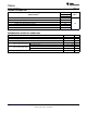
ABSOLUTE MAXIMUM RATINGS
over operating free-air temperature range (unless otherwise noted)
VALUE UNIT
V
IN
Input voltage range –0.3 to 6 V
V
OUT
Output voltage range VIN + 0.3 V
V
ON
Input voltage range –0.3 to 6 V
Maximum continuous power dissipation @ 25°C 463
P
MAX
Maximum continuous power dissipation @ 70°C 254 mW
Maximum continuous power dissipation @ 85°C 185
I
MAX
Maximum continuous operating current 2 A
T
A
Operating free-air temperature range –40 to 85 °C
T
J
Maximum junction temperature 125 °C
T
STG
Storage temperature range –65 to 150 °C
Human-Body Model (HBM) (VIN, VOUT, GND
2000
pins)
ESD Electrostatic discharge protection V
Charged-Device Model (CDM) (VIN, VOUT, ON,
1000
GND pins)
Copyright © 2011, Texas Instruments Incorporated Submit Documentation Feedback 3
Product Folder Link(s) :TPS22929