
Datasheet


Power
Supply
ON
OFF
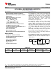
TPS22930
VIN VOUT
R
L
C
L
GND
ON
GND
C
IN
TPS22930
www.ti.com
SLVSBL3 –NOVEMBER 2012
ULTRA SMALL, LOW RESISTANCE LOAD SWITCH
Check for Samples: TPS22930
1
FEATURES
DESCRIPTION
The TPS22930 is a small, low R
ON
load switch with
• Integrated Single Channel Load Switch
controlled turn on. The device contains a P-channel
• Ultra Small CSP-4 Package (0.9mm × 0.9mm,
MOSFET that can operate over an input voltage
0.5mm pitch)
range of 1.4V to 5.5V. The switch is controlled by an
• Input Voltage Range: 1.4V to 5.5V
on/off input (ON), which is capable of interfacing
directly with low-voltage control signals. The
• Ultra Low R
ON
Resistance
TPS22930 is active high enable.
– R
ON
= 35mΩ at V
IN
= 5V
The TPS22930 device provides circuit breaker
– R
ON
= 36mΩ at V
IN
= 3.6V
functionality by disabling the body diode during
– R
ON
= 49mΩ at V
IN
= 1.8V
reverse voltage (also known as reverse current)
• 2A Maximum Continuous Switch Current
situations. Reverse current protection is active only
when the power-switch is disabled (off). The device
• Low Quiescent Current (< 3µA)
disengages the body diode when the output voltage
• Low Control Input Threshold Enables Use of
(V
OUT
) is driven higher than the input (V
IN
) to stop the
1.2V/1.8V/2.5V/3.3V Logic
flow of current towards the input side of the switch.
Additionally, under-voltage lockout (UVLO) protection
• Controlled Slew Rate
turns the switch off if the input voltage is too low.
• Under Voltage Lockout
The slew rate of the device is internally controlled in
• Reverse Current Protection When Disabled
order to avoid inrush current.
APPLICATIONS
The TPS22930 is available in an ultra-small, space-
saving 4-pin CSP package and is characterized for
• Smartphone / Wireless Handsets
operation over the free-air temperature range of
• Portable Industrial / Medical Equipment
–40°C to 85°C.
• Portable Media Players
• Point of Sales Terminals
• GPS Navigation Devices
• Digital Cameras
• Portable Instrumentation
Figure 1. Typical Application
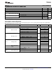
Feature List
RON (typ) at Rise Time at Quick Output Maximum
Device Enable
4.2V 4.2V (typ) Discharge
(1)
Continuous Current
TPS22930A 35mΩ 5.4µs No 2A Active High
(1) This feature discharges output of the switch to GND through a resistor, preventing the output from floating when the pass FET is
disabled
1
Please be aware that an important notice concerning availability, standard warranty, and use in critical applications of
Texas Instruments semiconductor products and disclaimers thereto appears at the end of this data sheet.
PRODUCTION DATA information is current as of publication date.
Copyright © 2012, Texas Instruments Incorporated
Products conform to specifications per the terms of the Texas
Instruments standard warranty. Production processing does not
necessarily include testing of all parameters.