
Datasheet
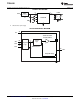
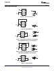


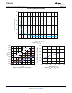

Laser Marking View
Bump View
C
B
2 1
A
C
B
1 2
A
TPS22932B
www.ti.com
SLVS802B –AUGUST 2009–REVISED AUGUST 2013
LOW INPUT VOLTAGE, ULTRA-LOW r
ON
LOAD SWITCH
WITH CONFIGURABLE ENABLE LOGIC AND CONTROLLED SLEW-RATE
Check for Samples: TPS22932B
1
FEATURES
APPLICATIONS
• Input Voltage: 1.1 V to 3.6 V • PDAs
• Ultra-Low ON Resistance • Cell Phones
– r
ON
= 55 mΩ at V
IN
= 3.6 V • GPS Devices
– r
ON
= 65 mΩ at V
IN
= 2.5 V • MP3 Players
– r
ON
= 75 mΩ at V
IN
= 1.8 V • Digital Cameras
– r
ON
= 115 mΩ at V
IN
= 1.2 V • Peripheral Ports
• 500-mA Maximum Continuous Switch Current • Portable Instrumentation
• Quiescent Current < 1 μA
DESCRIPTION
• Shutdown Current < 1 μA
TPS22932B is a low r
ON
load switch with controlled
• Low Control Threshold Allows Use of 1.2-
turn on. It contains an ultra-low r
ON
P-channel
V/1.8-V/2.5-V/3.3-V Logic
MOSFET that can operate over an input voltage
• Configurable Enable Logic
range of 1.1 V to 3.6 V.
• Controlled Slew Rate to Avoid Inrush
The switch is controlled by eight patterns of 3-bit
Currents: 165 μs at 1.8 V
input. The user can choose the logic functions MUX,
AND, OR, NAND, NOR, inverter, and non-inverter. All
• ESD Performance Tested Per JESD 22
inputs can be connected to V
IN
or GND. The control
– 2000-V Human-Body Model
pins can be connected to low voltage GPIOs allowing
(A114-B, Class II)
it to be controlled by whatever 1.2-V, 1.8-V, 2.5-V, or
– 1000-V Charged-Device Model (C101)
3.3-V logic signals while keeping extremely low
quiescent current.
• Six-Terminal Wafer Chip Scale Package
(DSBGA)
A 120-Ω on-chip load resistor is available for output
– 0.8 mm × 1.2 mm,
quick discharge when the switch is turned off. The
rise time (slew rate) of the device is internally
0.4-mm Pitch, 0.5-mm Height
controlled to avoid inrush current: the rise time of
TPS22932B is 165 μs.
TPS22932B is available in a space-saving 6-terminal
DSBGA (YFP with 0.4-mm pitch). The device is
characterized for operation over the free-air
temperature range of –40°C to 85°C.
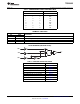
r
ON
AT 1.8 V SLEW RATE QUICK OUTPUT MAX OUTPUT
DEVICE ENABLE
(TYP) (TYP AT 3.3 V) DISCHARGE
(1)
CURRENT
TPS22932B 75 mΩ 165 μs Yes 500 mA Active high
(1) This feature discharges the output of the switch to ground through a 120-Ω resistor, preventing the output from floating.
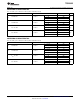
Table 1. TERMINAL ASSIGNMENTS
YFP PACKAGE
C ON2 ON3
B ON1 GND
A V
IN
V
OUT
2 1
1
Please be aware that an important notice concerning availability, standard warranty, and use in critical applications of
Texas Instruments semiconductor products and disclaimers thereto appears at the end of this data sheet.
PRODUCTION DATA information is current as of publication date.
Copyright © 2009–2013, Texas Instruments Incorporated
Products conform to specifications per the terms of the Texas
Instruments standard warranty. Production processing does not
necessarily include testing of all parameters.