
Datasheet
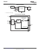


ON1
Y
ON2
ON3
4
TPS22932B
www.ti.com
SLVS802B –AUGUST 2009–REVISED AUGUST 2013
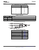
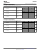
Table 2. CONFIGURABLE LOGIC FUNCTION TABLE
INPUTS SWITCH CONTROL
ON3 ON2 ON1 Y
L L L OFF
L L H OFF
L H L ON
L H H ON
H L L OFF
H L H ON
H H L OFF
H H H ON
TERMINAL FUNCTIONS
TERMINAL
DESCRIPTION
NO. NAME
A1 V
OUT
Switch output
A2 V
IN
Switch input, bypass this input with a ceramic capacitor to ground
B1 GND Ground
B2, C2, C1 ON1, ON2, ON3 Switch control input, active high - Do not leave floating
LOGIC DIAGRAM (POSITIVE LOGIC)
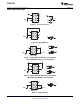
Table 3. FUNCTION SELECTION TABLE
LOGIC FUNCTION FIGURE NO.
2-to-1 data selector Figure 1
2-input AND gate Figure 2
2-input OR gate with one inverted input Figure 3
2-input NAND gate with one inverted input Figure 3
2-input AND gate with one inverted input Figure 4
2-input NOR gate with one inverted input Figure 4
2-input OR gate Figure 5
Inverter Figure 6
Noninverted buffer Figure 7
Copyright © 2009–2013, Texas Instruments Incorporated Submit Documentation Feedback 3
Product Folder Links: TPS22932B