
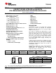
Datasheet
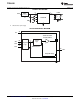
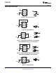


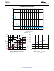

Y
ON3
GND
V
OUT
V
IN
ON2
ON1
GND
Bump View
A
A
Y
ON3
GND
V
OUT
V
IN
/V
CC
V
IN
ON2
ON1
GND
Bump View
A
A
TPS22932B
www.ti.com
SLVS802B –AUGUST 2009–REVISED AUGUST 2013
Figure 6. Inverter
Figure 7. Noninverted Buffer
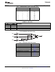
ABSOLUTE MAXIMUM RATINGS
(1)
MIN MAX UNIT
V
IN
Input voltage range –0.3 4 V
V
OUT
Output voltage range V
IN
+ 0.3 V
P Power dissipation at T
A
= 25°C 0.8 W
I
MAX
Maximum continuous switch current 500 mA
T
A
Operating free-air temperature range –40 85 °C
T
stg
Storage temperature range –65 150 °C
T
lead
Maximum lead temperature (10-s soldering time) 300 °C
Human-Body Model (HBM) 2000
ESD Electrostatic discharge protection V
Charged Device Model (CDM) 1000
(1) Stresses beyond those listed under absolute maximum ratings may cause permanent damage to the device. These are stress ratings
only, and functional operation of the device at these or any other conditions beyond those indicated under Recommended Operating
Conditions is not implied. Exposure to absolute-maximum-rated conditions for extended periods may affect device reliability.
THERMAL IMPEDANCE RATINGS
TYP UNIT
θ
JA
Package thermal impedance
(1)
YFP package 155 °C/W
(1) The package thermal impedance is calculated in accordance with JESD 51-7.
RECOMMENDED OPERATING CONDITIONS
MIN MAX UNIT
I
OUT
Output current 500 mA
V
IN
Input voltage range 1.1 3.6 V
V
OUT
Output voltage range V
IN
C
IN
Input capacitor 1
(1)
μF
(1) See Application Information.
Copyright © 2009–2013, Texas Instruments Incorporated Submit Documentation Feedback 5
Product Folder Links: TPS22932B