
Datasheet
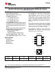
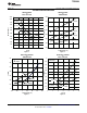
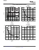

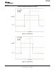
Table Of Contents
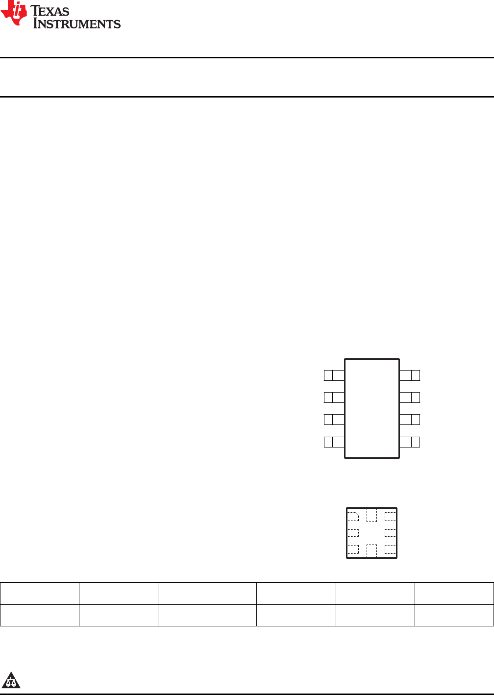
RSE PACKAGE
(TOP VIEW)
V
IN2
V
OUT1
V
IN1
ON1
SR
ON2
GND
V
OUT2
7
1
6
2
8
5
3
4
DCN PACKAGE
(TOP VIEW)
8
1
6
3
7
2
V
IN1
ON2
ON1
V
IN2
5
4
V
OUT1
GND
SR
V
OUT2
TPS22960
www.ti.com
SLVS914B –APRIL 2009–REVISED AUGUST 2013
LOW INPUT VOLTAGE, DUAL LOAD SWITCH WITH CONTROLLED TURN-ON
Check for Samples: TPS22960
1
FEATURES
DESCRIPTION
The TPS22960 is a small low-r
ON
dual load switch
• Integrated Dual Load Switch
with controlled turn on. The devices contain two P-
• Input Voltage Range: 1.62 V to 5.5 V
channel MOSFETs that can operate over an input
• Low ON-State Resistance
voltage range of 1.62 V to 5.5 V. Each switch is
controlled by an on/off input (ON1 and ON2), which is
– r
ON
= 342 mΩ at V
IN
= 5.5 V
capable of interfacing directly with low-voltage control
– r
ON
= 435 mΩ at V
IN
= 3.3 V
signals. In TPS22960 a 85-Ω on-chip load resistor is
– r
ON
= 523 mΩ at V
IN
= 2.5 V
added for output quick discharge when switch is
turned off.
– r
ON
= 737 mΩ at V
IN
= 1.8 V
• 500-mA Maximum Continuous Switch Current
The rise time (slew-rate) of the device is internally
controlled in order to avoid inrush current and can be
• Low Quiescent Current and Shutdown Current
slowed down if needed using the SR pin: TPS22960
• Controlled Switch Output Rise Time: 75 μs or
features a 75 μs rise time with the SR pin tied to
660 μs
ground and 660 μs with the SR pin tied to high.
• Integrated Quick Output Discharge Transistor
The TPS22960 is available in a space-saving 8-pin
• ESD Performance Tested Per JESD 22
μQFN package and in an 8-pin SOT package. It is
– 2000-V Human-Body Model
characterized for operation over the free-air
temperature range of –40°C to 85°C.
(A114-B, Class II)
– 1000-V Charged-Device Model (C101)
• 8-Pin SOT (DCN) Package: 3 mm × 3 mm
• 8-Pin μQFN (RSE) Package: 1.5 mm × 1.5 mm
APPLICATIONS
• GPS Devices
• Cell Phones/PDAs
• MP3 Players
• Digital Cameras
r
ON
AT 3.3 V SLEW RATE AT 3.3 V QUICK OUTPUT MAX OUTPUT
DEVICE ENABLE
(TYP) (TYP) DISCHARGE
(1)
CURRENT
75 μs with SR = low
TPS22960 435 mΩ Yes 500 mA Active High
660 μs with SR = high
(1) This feature discharges the output of the switch to ground through a 85-Ω resistor, preventing the output from floating.
1
Please be aware that an important notice concerning availability, standard warranty, and use in critical applications of
Texas Instruments semiconductor products and disclaimers thereto appears at the end of this data sheet.
PRODUCTION DATA information is current as of publication date.
Copyright © 2009–2013, Texas Instruments Incorporated
Products conform to specifications per the terms of the Texas
Instruments standard warranty. Production processing does not
necessarily include testing of all parameters.