
Datasheet


SLUS536C − AUGUST 2002 − REVISED AUGUST 2004
FEATURES
D Wide Input Supply Range: −20 V to −80 V
D Transient Rating to −100 V
D Programmable Current Limit
D Programmable Current Slew Rate
D Programmable UV/OV Thresholds/Hysteresis
D Debounced Insertion Detection Inputs
D Open-Drain Power Good (PG) Output
D Fault Timer to Eliminate Nuisance Trips
D Open-Drain Fault Output (FAULT)
D Enable Input (EN)
D 14-Pin TSSOP package
D 44-Pin TSSOP Package for
Creapage/Clearance
APPLICATIONS
D −48-V Distributed Power Systems
D Central Office Switching
D Wireless Base Station
DESCRIPTION
The TPS2392 and TPS2393 integrated circuits are hot
swap power managers optimized for use in nominal
−48-V systems. They operate with supply voltage
ranges from −20-V to −80-V, and are rated to withstand
spikes to −100 V. In conjunction with an external
N-channel FET and sense resistor, they can be used to
enable live insertion of plug-in cards and modules in
powered systems. Each device provides load current
slew rate control and peak magnitude limiting.
Undervoltage and overvoltage shutdown thresholds
are easily programmed via a three-resistor divider
network. In addition, two active-low, debounced inputs
provide plug-in insertion detection. A power good (PG)
output enables downstream converters. The TPS2392
and TPS2393 also provide the basic hot swap functions
of electrical isolation of faulty cards, filtered protection
against nuisance overcurrent trips, and single-line fault
reporting. The 44-pin part supports designs where
telecomm creepage and clearance requirements must
be followed.
The TPS2392 latches off in response to current faults,
while the TPS2393 periodically retries the load in the
event of a fault.
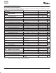
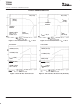
UDG−02098
D1
BAS19
C2
0.1 µF
R3
3.92 kΩ
1%
R2
4.99 kΩ
1%
R1
200 kΩ
1%
R4
20 mΩ
1/4, 1%
R6
10 kΩ
R5
100
kΩ
C4
100 µF
100 V
C
OUT
= 32.8 V
= 30.8 V
= 72.6 V
V
UV
V
UV
V
OV
GATE
1
2
3
4
5
6
7
14
13
12
11
10
9
8
UVLO
INSA
INSB
FAULT
EN
FLTTIME
OVLO
DRAINSNS
ISENS
IRAMP −VIN
PG
RTN
TPS2392/TPS2393
VOUT+
VOUT−
VIN+
VIN−
DC/DC
CONVERTER
EN
V
DD
C3
1500 pF
VOUT+
VOUT−
GND
C1
3900 pF
−48V
Q1
IRF530
D2
5.6 V
!"# $ %&'# "$ (&)*%"# +"#', +&%#$
%! # $('%%"#$ (' #-' #'!$ '."$ $#&!'#$ $#"+"+ /""#0,
+&%# (%'$$1 +'$ # '%'$$"*0 %*&+' #'$#1 "** (""!'#'$,
.
Please be aware that an important notice concerning availability, standard warranty, and use in critical applications of Texas Instruments
semiconductor products and disclaimers thereto appears at the end of this data sheet.
www.ti.com
Copyright 2004, Texas Instruments Incorporated