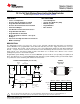
TPS24710, TPS24711 TPS24712, TPS24713 www.ti.com SLVSAL2E – JANUARY 2011 – REVISED NOVEMBER 2013 2.5-V to 18-V High-Efficiency Power-Limiting Hot-Swap Controller Check for Samples: TPS24710, TPS24711, TPS24712, TPS24713 FEATURES APPLICATIONS • • • • • • • • • • • • • • 1 • • 2.
TPS24710, TPS24711 TPS24712, TPS24713 SLVSAL2E – JANUARY 2011 – REVISED NOVEMBER 2013 www.ti.com This integrated circuit can be damaged by ESD. Texas Instruments recommends that all integrated circuits be handled with appropriate precautions. Failure to observe proper handling and installation procedures can cause damage. ESD damage can range from subtle performance degradation to complete device failure.
TPS24710, TPS24711 TPS24712, TPS24713 www.ti.com SLVSAL2E – JANUARY 2011 – REVISED NOVEMBER 2013 RECOMMENDED OPERATING CONDITIONS over operating free-air temperature range (unless otherwise noted) MIN Input voltage range SENSE, VCC EN, FLT, FLTb, PG, PGb, OUT NOM MAX 2.5 18 0 18 UNIT V Sink current FLT, FLTb, PG, PGb 0 2 mA Resistance PROG 4.
TPS24710, TPS24711 TPS24712, TPS24713 SLVSAL2E – JANUARY 2011 – REVISED NOVEMBER 2013 www.ti.com ELECTRICAL CHARACTERISTICS (continued) –40°C ≤ TJ ≤ 125°C, VCC = 12 V, VEN = 3 V, and RPROG = 50 kΩ to GND. All voltages referenced to GND, unless otherwise noted. PARAMETER CONDITIONS MIN NOM MAX UNIT VTIMER = 2 V 8 10 12 µA VEN = 0 V, VTIMER = 2 V 2 4.5 7 mA Upper threshold voltage 1.30 1.35 1.40 V Lower threshold voltage 0.33 0.35 0.
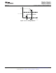
TPS24710, TPS24711 TPS24712, TPS24713 www.ti.com SLVSAL2E – JANUARY 2011 – REVISED NOVEMBER 2013 VGATE 50% VVCC – VSENSE 50% 0 Time t(prf50-50) T0495-01 Figure 3.
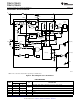
TPS24710, TPS24711 TPS24712, TPS24713 SLVSAL2E – JANUARY 2011 – REVISED NOVEMBER 2013 www.ti.com FUNCTIONAL BLOCK DIAGRAM M1 VIN RSENSE SENSE RGATE GATE 8 OUT 7 6 60 mV DC + Charge Pump – RSET Servo Amplifier RIMON = 27 RSET Inrush Latch + 30 µA + 9 – VCC Fast Comparator Gate Comparator – VCC 5.9 V 11 mA 1-shot S Q R Q + – 0~60 µA RIMON + A – æ KpA ö , 675 mV ÷ è B ø Main Opamp in Inrush Min ç B + PROG – 3 RPROG OUT DC UVLO + 2.32 V 2.
TPS24710, TPS24711 TPS24712, TPS24713 www.ti.com SLVSAL2E – JANUARY 2011 – REVISED NOVEMBER 2013 PIN FUNCTIONS (continued) NAME PINS TPS24710/11 TPS24712/13 I/O DESCRIPTION Active-high, open-drain power good indicator. Status is determined by the voltage across the MOSFET. PG - 1 PGb 1 - PROG 3 3 I Power-limiting programming pin. A resistor from this pin to GND sets the maximum power dissipation for the FET. SENSE 8 8 I Current sensing input for resistor shunt from VCC to SENSE.
TPS24710, TPS24711 TPS24712, TPS24713 SLVSAL2E – JANUARY 2011 – REVISED NOVEMBER 2013 www.ti.com – VVCC drops below the UVLO threshold 2. GATE is pulled down by a 1 A current source for 13.5 µs when a hard output short circuit occurs and V(VCC – SENSE) is greater than 60 mV, i.e., the fast-trip shutdown threshold. After fast-trip shutdown is complete, an 11-mA sustaining current ensures that the external MOSFET remains off. 3.
TPS24710, TPS24711 TPS24712, TPS24713 www.ti.com PLIM < SLVSAL2E – JANUARY 2011 – REVISED NOVEMBER 2013 TJ(MAX) - TC(MAX) RθJC(MAX) (2) where TJ(MAX) is the maximum desired transient junction temperature and TC(MAX) is the maximum case temperature prior to a start or restart. RӨJC(MAX) is the junction-to-case thermal impedance of the pass MOSFET M1 in units of °C/W. Both TJ(MAX) and TC(MAX) are in °C. SENSE: This pin connects to the negative terminal of RSENSE.
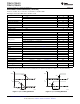
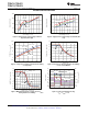
TPS24710, TPS24711 TPS24712, TPS24713 SLVSAL2E – JANUARY 2011 – REVISED NOVEMBER 2013 www.ti.com TYPICAL CHARACTERISTICS 5 1200 T = 125°C 1000 T = 25°C Supply Current (µA) Supply Current (µA) 4 T = 125°C 800 T = –40°C T = 25°C 3 2 T = –40°C 600 1 400 0 4 2 6 8 10 12 14 Input Voltage, VVCC (V) 16 18 0 20 Figure 5. Supply Current vs Input Voltage at Normal Operation (EN = High) 0 4 2 6 8 10 12 14 Input Voltage, VVCC (V) 16 18 20 Figure 6.
TPS24710, TPS24711 TPS24712, TPS24713 www.ti.com SLVSAL2E – JANUARY 2011 – REVISED NOVEMBER 2013 0.7 0.2 T = –40°C Gate Current (A) 0.6 0.15 T = 25°C 0.5 0.1 0.4 0.05 0.3 0 V(VCC – SENSE) T = 125°C 0.2 –0.05 0.1 –0.1 0 –0.15 –0.1 –0.2 VVCC = 3.3 V –0.2 –10 0 10 20 40 30 –0.25 Gate Voltage Referenced to GND, VGATE (V) 0.25 Voltage, V(VCC – SENSE) (V) TYPICAL CHARACTERISTICS (continued) 0.9 Time (µs) Figure 11. Gate Current During Fast Trip, VVCC = VGATE = 3.
TPS24710, TPS24711 TPS24712, TPS24713 SLVSAL2E – JANUARY 2011 – REVISED NOVEMBER 2013 www.ti.com TYPICAL CHARACTERISTICS (continued) 64 PG Falling and PGb Rising Fast-Trip Threshold Voltage (mV) V(SENSE – OUT) Threshold Voltage (mV) 240 220 200 180 PG Rising and PGb Falling 160 140 –50 10 –20 40 70 Temperature (°C) 100 140 120 VVCC = 18 V VVCC = 2.5 V 100 80 VVCC = 12 V 60 –50 10 –20 40 70 Temperature (°C) 100 130 Figure 19.
TPS24710, TPS24711 TPS24712, TPS24713 www.ti.com SLVSAL2E – JANUARY 2011 – REVISED NOVEMBER 2013 TYPICAL CHARACTERISTICS (continued) 10.2 Timer Sourcing Current (µA) Timer Lower Threshold Voltage (V) 0.365 VVCC = 18 V 0.362 VVCC = 12 V 0.36 –20 10 40 70 Temperature (°C) 10 VVCC = 18 V VVCC = 12 V 9.9 9.8 9.7 VVCC = 2.5 V 9.6 VVCC = 2.5 V 0.357 –50 10.1 100 9.5 –50 130 Figure 23.
TPS24710, TPS24711 TPS24712, TPS24713 SLVSAL2E – JANUARY 2011 – REVISED NOVEMBER 2013 www.ti.com SYSTEM OPERATION INTRODUCTION The TPS24710/11/12/13 provides all the features needed for a positive hot-swap controller.
TPS24710, TPS24711 TPS24712, TPS24713 www.ti.com SLVSAL2E – JANUARY 2011 – REVISED NOVEMBER 2013 Figure 26. Inrush Mode at Hot-Swap Circuit Insertion INRUSH OPERATION After TPS24710/11/12/13 initialization is complete (as described in the Board Plug-In section) and EN is active, GATE is enabled (VGATE starts increasing). When VGATE reaches the MOSFET M1 gate threshold, a current flows into the downstream bulk storage capacitors.
TPS24710, TPS24711 TPS24712, TPS24713 SLVSAL2E – JANUARY 2011 – REVISED NOVEMBER 2013 www.ti.com dissipated within the MOSFET, labeled FET PWR, remaining substantially constant during this period of operation, which ends when the current through the MOSFET reaches the current limit ILIM.
TPS24710, TPS24711 TPS24712, TPS24713 www.ti.com SLVSAL2E – JANUARY 2011 – REVISED NOVEMBER 2013 Figure 28. Circuit Breaker Mode During Over Load Condition ILIMIT M1 RSENSE RGATE VCC 9 RSET SENSE GATE 8 7 OUT 6 + 60 mV + Server Amplifier – – Fast Trip Comparator A1 60 μA + 675 mV PROG RIMON VCP – Current Limit Amp 3 RPROG A2 30 μA + B0439-02 Figure 29.
TPS24710, TPS24711 TPS24712, TPS24713 SLVSAL2E – JANUARY 2011 – REVISED NOVEMBER 2013 www.ti.com Figure 30. Current Limit During Output Load Short Circuit Condition (Overview) Figure 31.
TPS24710, TPS24711 TPS24712, TPS24713 www.ti.com SLVSAL2E – JANUARY 2011 – REVISED NOVEMBER 2013 AUTOMATIC RESTART The TPS24711/13 automatically initiates a restart after a fault has caused it to turn off the external MOSFET M1. Internal control circuits use CT to count 16 cycles before re-enabling M1 as shown in Figure 32 (TPS24711). This sequence repeats if the fault persists. The timer has a 1 : 1 charge-to-discharge current ratio.
TPS24710, TPS24711 TPS24712, TPS24713 SLVSAL2E – JANUARY 2011 – REVISED NOVEMBER 2013 www.ti.com Figure 33. Latch After Overload Fault PG, FLT, PGb, FLTb, AND TIMER OPERATIONS The open-drain PG/PGb (PG is for TPS24712/13 and PGb is for TPS24710/11) output provides a deglitched end-of-inrush indication based on the voltage across M1. PG/PGb is useful for preventing a downstream dc/dc converter from starting while its input capacitor COUT is still charging.
TPS24710, TPS24711 TPS24712, TPS24713 www.ti.com SLVSAL2E – JANUARY 2011 – REVISED NOVEMBER 2013 activation voltage (see the Inrush Operation section). If V(GATE – VCC) does not reach the timer activation voltage before TIMER reaches 1.35 V, then the TPS24710/11/12/13 disables the external MOSFET M1. After the MOSFET turns off, the timer goes into either latch mode (TPS24710/12) or retry mode (TPS24711/13). 2.
TPS24710, TPS24711 TPS24712, TPS24713 SLVSAL2E – JANUARY 2011 – REVISED NOVEMBER 2013 www.ti.com DESIGN EXAMPLE: POWER-LIMITED START-UP This design example assumes a 12-V system voltage with an operating tolerance of ±2 V. The rated load current is 10 A, corresponding to a dc load of 1.2 Ω. If the current exceeds 12 A, then the controller should shut down and then attempt to restart. Ambient temperatures may range from 20°C to 50°C. The load has a minimum input capacitance of 470 μF.
TPS24710, TPS24711 TPS24712, TPS24713 www.ti.com SLVSAL2E – JANUARY 2011 – REVISED NOVEMBER 2013 Next select the on resistance of the transistor, rDS(on). The maximum on-resistance must not generate a voltage greater then the minimum power-good threshold voltage of 140 mV. Assuming a current limit of 12 A, a maximum rDS(on) of 11.67 mΩ is required. Also consider the effect of rDS(on) upon the maximum operating temperature TJ(MAX) of the MOSFET.
TPS24710, TPS24711 TPS24712, TPS24713 SLVSAL2E – JANUARY 2011 – REVISED NOVEMBER 2013 www.ti.com STEP 4. Choose Output Voltage Rising Time, tON, CT The maximum output voltage rise time, tON, set by the timer capacitor CT must suffice to fully charge the load capacitance COUT without triggering the fault circuitry. Equation 10 defines tON for two possible inrush cases.
TPS24710, TPS24711 TPS24712, TPS24713 www.ti.com SLVSAL2E – JANUARY 2011 – REVISED NOVEMBER 2013 IDS – Drain-to-Source Current – A 1k 100 1ms 10 10ms 100ms Area Limited by RDS(on) 1 1s 0.1 Single Pulse RθJA = 94ºC/W (min Cu) 0.01 0.01 0.1 DC 1 10 VDS – Drain-to-Source Voltage – V 100 G009 Figure 35. CSD16403Q5 SOA Curve STEP 5.
TPS24710, TPS24711 TPS24712, TPS24713 SLVSAL2E – JANUARY 2011 – REVISED NOVEMBER 2013 www.ti.com To select the gate capacitance, use Equation 15. IGATE is the nominal gate charge current. This equation assumes that the MOSFET CGD is the controlling element as the gate and output voltage rise. CGD is non-linear with applied VDG. An averaged estimate may be made using the MOSFET VGS vs QG curve. Divide the charge accumulated during the plateau region by the plateau VGS to get CRS.
TPS24710, TPS24711 TPS24712, TPS24713 www.ti.com SLVSAL2E – JANUARY 2011 – REVISED NOVEMBER 2013 Bypass Capacitors It is a good practice to provide low-impedance ceramic capacitor bypassing of the VCC and OUT pins. Values in the range of 10 nF to 1 µF are recommended. Some system topologies are insensitive to the values of these capacitors; however, some are not and require minimization of the value of the bypass capacitor.
TPS24710, TPS24711 TPS24712, TPS24713 SLVSAL2E – JANUARY 2011 – REVISED NOVEMBER 2013 www.ti.com REVISION HISTORY Changes from Revision A (March 2011) to Revision B • Page Corrected voltage values shown in block diagram ............................................................................................................... 6 Changes from Revision B (April 2011) to Revision C Page • Changed in PGb: from: 140V/340mV, to:170mV / 240mV .............................................................
PACKAGE OPTION ADDENDUM www.ti.
PACKAGE OPTION ADDENDUM www.ti.com (4) 19-Nov-2013 There may be additional marking, which relates to the logo, the lot trace code information, or the environmental category on the device. (5) Multiple Device Markings will be inside parentheses. Only one Device Marking contained in parentheses and separated by a "~" will appear on a device. If a line is indented then it is a continuation of the previous line and the two combined represent the entire Device Marking for that device.
PACKAGE MATERIALS INFORMATION www.ti.com 19-Nov-2013 TAPE AND REEL INFORMATION *All dimensions are nominal Device Package Package Pins Type Drawing SPQ Reel Reel A0 Diameter Width (mm) (mm) W1 (mm) B0 (mm) K0 (mm) P1 (mm) W Pin1 (mm) Quadrant TPS24710DGSR VSSOP DGS 10 2500 330.0 12.4 5.3 3.4 1.4 8.0 12.0 Q1 TPS24711DGSR VSSOP DGS 10 2500 330.0 12.4 5.3 3.4 1.4 8.0 12.0 Q1 TPS24712DGSR VSSOP DGS 10 2500 330.0 12.4 5.3 3.4 1.4 8.0 12.
PACKAGE MATERIALS INFORMATION www.ti.com 19-Nov-2013 *All dimensions are nominal Device Package Type Package Drawing Pins SPQ Length (mm) Width (mm) Height (mm) TPS24710DGSR VSSOP DGS 10 2500 358.0 335.0 35.0 TPS24711DGSR VSSOP DGS 10 2500 358.0 335.0 35.0 TPS24712DGSR VSSOP DGS 10 2500 358.0 335.0 35.0 TPS24713DGSR VSSOP DGS 10 2500 358.0 335.0 35.
IMPORTANT NOTICE Texas Instruments Incorporated and its subsidiaries (TI) reserve the right to make corrections, enhancements, improvements and other changes to its semiconductor products and services per JESD46, latest issue, and to discontinue any product or service per JESD48, latest issue. Buyers should obtain the latest relevant information before placing orders and should verify that such information is current and complete.