
Datasheet

SLVS132F − NOVEMBER 1995 − REVISED OCTOBER 2004
1
www.ti.com
D Industry-Standard Driver Replacement
D 25-ns Max Rise/Fall Times and 40-ns Max
Propagation Delay − 1-nF Load, V
CC
= 14 V
D 2-A Peak Output Current, V
CC
= 14 V
D 5-µA Supply Current — Input High or Low
D 4-V to 14-V Supply-Voltage Range; Internal
Regulator Extends Range to 40 V (TPS2811,
TPS2812, TPS2813)
D −40°C to 125°C Ambient-Temperature
Operating Range
description
The TPS28xx series of dual high-speed MOSFET
drivers are capable of delivering peak currents of 2 A
into highly capacitive loads. This performance is
achieved with a design that inherently minimizes
shoot-through current and consumes an order of
magnitude less supply current than competitive
products.
The TPS2811, TPS2812, and TPS2813 drivers include
a regulator to allow operation with supply inputs
between 14 V and 40 V. The regulator output can power
other circuitry, provided power dissipation does
not exceed package limitations. When the regulator is not required, REG_IN and REG_OUT can be left disconnected
or both can be connected to V
CC
or GND.
The TPS2814 and the TPS2815 have 2-input gates that give the user greater flexibility in controlling the MOSFET.
The TPS2814 has AND input gates with one inverting input. The TPS2815 has dual-input NAND gates.
TPS281x series drivers, available in 8-pin PDIP, SOIC, and TSSOP packages operate over a ambient temperature
range of −40°C to 125°C.
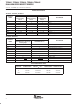
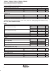
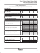
AVAILABLE OPTIONS
PACKAGED DEVICES
T
A
INTERNAL
REGULATOR
LOGIC FUNCTION
SMALL
OUTLINE
(D)
PLASTIC
DIP
(P)
TSSOP (PW)
−40°C
to
Yes
Dual inverting drivers
Dual noninverting drivers
One inverting and one noninverting driver
TPS2811D
TPS2812D
TPS2813D
TPS2811P
TPS2812P
TPS2813P
TPS2811PW
TPS2812PW
TPS2813PW
to
125°C
No
Dual 2-input AND drivers, one inverting input on each driver
Dual 2-input NAND drivers
TPS2814D
TPS2815D
TPS2814P
TPS2815P
TPS2814PW
TPS2815PW
The D package is available taped and reeled. Add R suffix to device type (e.g., TPS2811DR). The PW package is only available left-end
taped and reeled and is indicated by the R suffix on the device type (e.g., TPS2811PWR).
!"# $ %&'# "$ (&)*%"# +"#',
+&%#$ %! # $('%%"#$ (' #-' #'!$ '."$ $#&!'#$
$#"+"+ /""#0, +&%# (%'$$1 +'$ # '%'$$"*0 %*&+'
#'$#1 "** (""!'#'$,
Copyright 2002, Texas Instruments Incorporated
Please be aware that an important notice concerning availability, standard warranty, and use in critical applications of
Texas Instruments semiconductor products and disclaimers thereto appears at the end of this data sheet.
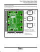
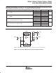
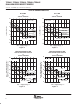
1
2
3
4
8
7
6
5
REG_IN
1IN
GND
2IN
REG_OUT
1OUT
V
CC
2OUT
TPS2811, TPS2812, TPS2813 ...D, P, AND PW
PACKAGES
(TOP VIEW)
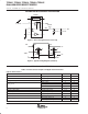
1
2
3
4
8
7
6
5
1IN1
1IN2
2IN1
2IN2
GND
1OUT
V
CC
2OUT
TPS2814 ...D, P, AND PW PACKAGES
(TOP VIEW)
1
2
3
4
8
7
6
5
1IN1
1IN2
2IN1
2IN2
GND
1OUT
V
CC
2OUT
TPS2815 ...D, P, AND PW PACKAGES
(TOP VIEW)